
Liquid crystal display device with improved switching means

Inactive Publication Date: 2010-01-14
FRANCE BREVETAB
View PDF9 Cites 1 Cited by
  • Summary
  • Abstract
  • Description
  • Claims
  • Application Information

AI Technical Summary

Benefits of technology

[0046]A second advantage of the present invention is decreasing or even making negative the addressing time between each line.
[0047]A third advantage of the present invention is improved control of the proportion of each texture in the same pixel when a level of grey in this pixel is to be created in this manner.
[0048]Other characteristics, aims and advantages of this present invention will appear on reading the detailed description which follows, and by referring to the appended drawings, which are provided by way of non-limiting examples and in which:
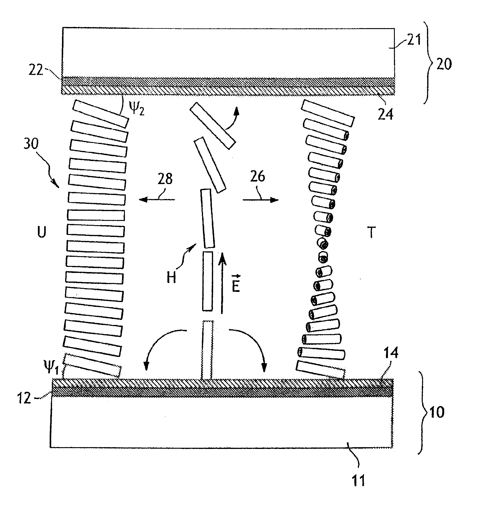
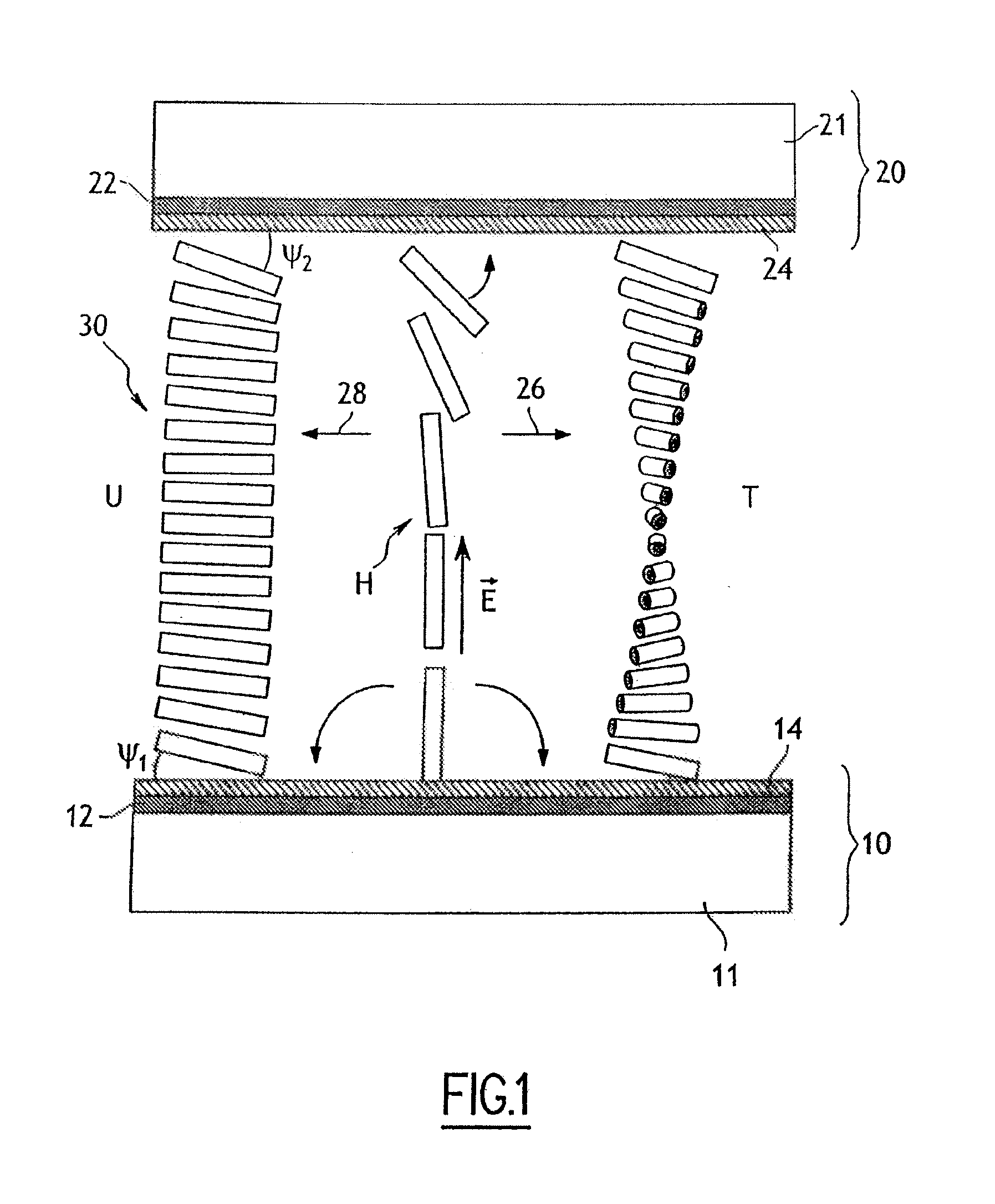
[0049]FIG. 1 shows the known operating principle of a bistable display of the BiNem type,
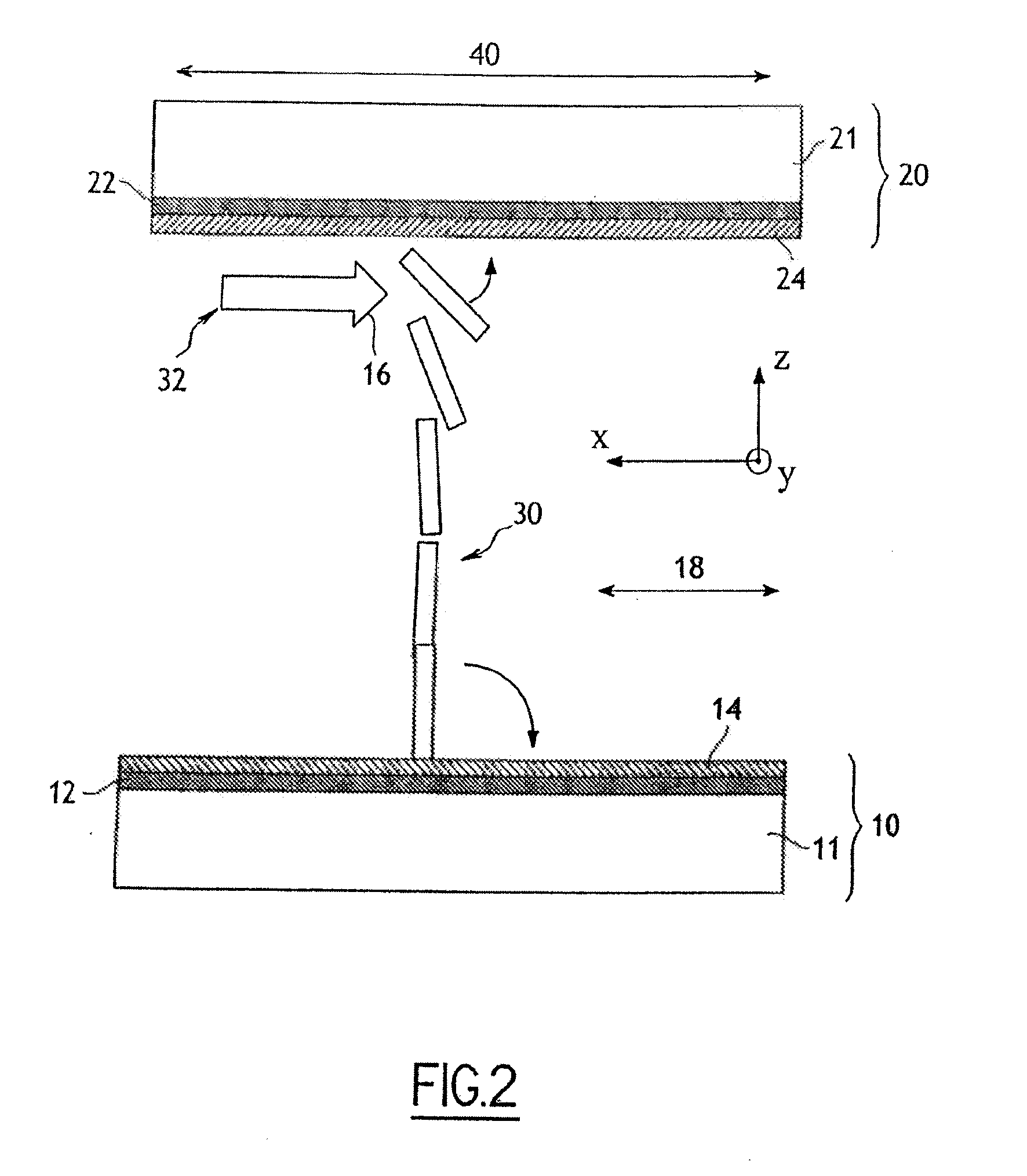
[0050]FIG. 2 represents the falling flow used for passage to texture T in such a display,
[0051]FIG. 3 illustrates the principle of conventional multiplexed passive addressing,

Problems solved by technology

By virtue of its operating principle, this type of display consumes energy in proportion to the number of image changes.
Thus, when the frequency of these changes reduces, the power necessary for the operation of the display tends toward zero.

Method used


Image

  • Liquid crystal display device with improved switching means
  • Liquid crystal display device with improved switching means
  • Liquid crystal display device with improved switching means

Examples


example 1 of embodiment

of the Invention

In Passive Addressing Acceleration of the Second Step of Addressing in Two Steps and Control of the Levels of Grey

[0084]Either a screen or a few lines of a passive multiplex matrix screen, addressed in two steps. The lines 52 are perpendicular to the brushing, thus perpendicular to the flows induced by movement of the molecules (orthogonal brushing). In reference to the second step of the display: the screen has been placed in texture T by the first step in the zone 100 to be switched. Switching is done on the line n. Switching of the pixel P (line n, column m) is studied.

[0085]At the start of the resulting switching, here by way of example of a voltage slot applied to a line n, lifting the molecules from the line n causes displacement of the liquid crystal by more than 100 nm. In the configuration of molecules illustrated in FIGS. 2 and 7, displacement is towards the positive x. This displacement creates near the line n−1 overpressure and near the line n+1 negative ...

example 2 of embodiment

of the Invention

Controlling Switching to U or T of the Pixels of the Line Activated During Line-by-Line Addressing (in One Step) in Passive Addressing

[0092]To undertake line-by-line addressing, according to the invention auxiliary signals applied to the adjacent pixels are used, and adjusted to consider their state (U, T or coexistence of both textures). A constraint is that the adjacent pixels located on the lines already recorded (n−1, n−2 . . . ) must not change state, and the auxiliary signal applied to these adjacent pixels must thus low in amplitude, that is, at least less than the breakage voltage. On the contrary, an auxiliary signal of strong amplitude can be applied to the lines along the line n to be recorded (lines not yet recorded with the new image, n+1, n+2 . . . ).

[0093]It is accordingly possible with an auxiliary signal line to lift then relax the molecules corresponding to the preceding lines and following the line n to be recorded, and use their rise and fall flow...

example 3 of embodiment

of the Invention

Rapid Addressing in Two Steps Using a Pixel Signal which does not break the anchorage for changing to T of Pixels that should Remain in T

[0094]In using the auxiliary flows of the adjacent pixels, the inventors have brought to light another variant of a rapid display process in black and white which saves on power.

[0095]This is a method in two steps. During the first step, the part of the screen to be displayed is put uniformly in T.

[0096]During the second step the display is composed line after line and the line activation signals can be simple slots. The amplitude V1 of the line activation signal VL is slightly less than the breakage value Vcass of the anchorage on the slave surface 10. The chronogram of these signals is shown in FIG. 16:

[0097]To change the pixel P(n, m) to U, the breakage is produced by a negative slot column signal illustrated in FIG. 16d: Vp=VL−Vc>Vcass. In this variant, it is not necessary for the falling edge of the column signal to be synchron...


PUM


Abstract

The invention relates to a method for controlling a liquid crystal display, comprising a matrix of pixels arranged in crossed lines and columns and in which a switch in the state of the liquid crystal molecules, controlled by application of an electric control signal between two electrodes (50, 52) enclosing each pixel, which brings about a flow in a given direction (18), the pixel addressing being carried out by a line by line addressing either in a single step or in two steps, the first step comprising a collective addressing of at least a part of the screen in a given single texture, followed by a second step of line by line addressing, characterised in comprising, for controlling the switching of at least some of the pixels (P), a step for application to at least one adjacent pixel (58) of auxiliary electric signals wherein, depending on the direction of flow of the pixel (P) the switching of which is to be controlled, the rising or falling fronts of the auxiliary signals are temporally advanced in relation to or simultaneous with the active falling front of the electric control signal with a time offset of between 0 and several tens of microseconds at ambient temperature, such as to promote the switching of said pixel (P) for control, said auxiliary electric signals being applied in the second step when the addressing is in two steps. The invention further relates to a display.

Description

TECHNICAL DOMAIN[0001]This present invention relates the field of liquid crystal displays.[0002]More precisely, this present invention concerns nematic bistable liquid crystal displays. It applies in particular to nematic bistable liquid crystal displays of which two stable textures differ by a twist of about 180°.AIM OF THE INVENTION[0003]The aim of this present invention is to improve the performance of the bistable display devices. In particular the objective of the invention is to improve, by the use of new means, the switching of states at the edges of the pixels.PRIOR ARTConventional LCD Displays[0004]The most widespread liquid crystal displays use a liquid crystal of the nematic type. They are composed of a liquid crystal layer placed between two plates. Each plate includes a substrate, often made of glass, on which have been deposited a conducting electrode and then a so-called anchor layer also called an alignment layer. The anchor layer exerts, on the adjacent liquid cryst...

Claims


Application Information

Patent Timeline
IPC IPC(8): G09G5/00G09G3/36
CPCG02F1/1391G09G3/36G09G2320/0209G09G3/3651G09G2300/0486G09G3/3622G02F1/139
Inventor MARTINOT-LAGARDE, PHILIPPEJOLY, STEPHANELAFFITTE, JEAN DENIS
Owner FRANCE BREVETAB
Learn More