Thin film transistor and display device including thin film transistor

a thin film transistor and display device technology, applied in the field of thin film transistors and display devices, can solve the problems of low field-effect mobility, vsec), low current, insufficient switching characteristics, etc., and achieve the effect of favorable electric characteristics and small shift amoun

Inactive Publication Date: 2009-11-26
SEMICON ENERGY LAB CO LTD
View PDF21 Cites 21 Cited by
  • Summary
  • Abstract
  • Description
  • Claims
  • Application Information

AI Technical Summary

Benefits of technology

[0026]In the thin film transistor having any of the above structures of the present invention, donor concentration in the microcrystalline semiconductor layer is preferably as high as possible and is preferably 1×10¹⁸ to 1×1021 cm−3 inclusive because the increase in donor concentration in the microcrystalline semiconductor layer leads to higher field-effect mobility, which allows high-speed operation.
[0030]The impurity semiconductor refers to a semiconductor in which a majority of carriers contributing to electrical conduction are supplied from an impurity element having one conductivity type which has been added to the semiconductor. The impurity element having one conductivity type is an element which can be a donor for supplying electrons as carriers or an acceptor for supplying holes as carriers. As a typical example of the donor, there is a Group 15 element in the periodic table. As a typical example of the acceptor, there is a Group 13 element in the periodic table. It is preferable to add an impurity element serving as a donor to the microcrystalline semiconductor layer, in order to improve the mobility of the microcrystalline semiconductor layer.
[0035]The microcrystalline semiconductor layer is provided in part of the channel formation region, and as for a certain distance of the channel formation region, carriers flow through the amorphous semiconductor layer. This structure can achieve a thin film transistor with excellent switching characteristics, that is, high on current and low off current.
[0037]A silicon nitride layer is provided as an insulating layer that is in contact with an amorphous semiconductor layer and a silicon oxynitride layer is provided as an insulating layer that is in contact with a microcrystalline semiconductor layer. Thus, a thin film transistor with low subthreshold swing, threshold voltage that does not shift (or the amount of the shift is small), and favorable electric characteristics can be provided.

Problems solved by technology

A thin film transistor in which an amorphous silicon layer is used for a channel formation region has problems of low field-effect mobility (about 0.4 to 0.8 cm2 / V·sec) and low on current.
However, the thin film transistor in which a microcrystalline silicon layer is used for a channel formation region has high off current along with high on current and therefore cannot have sufficient switching characteristics.
As a result, the manufacturing cost thereof becomes higher than those of the thin film transistor including an amorphous silicon layer and the thin film transistor including a microcrystalline silicon layer, which is a problem.
Moreover, there is also a problem in that when a laser annealing technique is used for the crystallization of the semiconductor layer, large-screen liquid crystal panels cannot be efficiently manufactured because a laser beam irradiation area is small.
However, a technique is not established yet for manufacturing thin film transistors capable of high-speed operation (for example, the aforementioned thin film transistor including a polycrystalline silicon layer) over a large-sized glass substrate with high productivity.
As for a technique for manufacturing thin film transistors capable of high-speed operation over a large-sized substrate, technique development has been advanced on a thin film transistor in which microcrystalline silicon is used for a channel formation region but its characteristics are not sufficient yet.

Method used


Image

  • Thin film transistor and display device including thin film transistor
  • Thin film transistor and display device including thin film transistor
  • Thin film transistor and display device including thin film transistor

Examples


embodiment 1

[0051]In Embodiment 1, examples of a structure of a thin film transistor according to an embodiment of the present invention will be described with reference to FIGS. 1A and 1B.

[0052]A thin film transistor illustrated in FIG. 1A includes a gate electrode layer 104 which is provided over a substrate 100; a first insulating layer 105 which is provided so as to cover the gate electrode layer 104; an impurity semiconductor layer 110a and an impurity semiconductor layer 110b forming a source region and a drain region, which are provided with a distance therebetween and which at least partly overlap with the gate electrode layer 104; a microcrystalline semiconductor layer 107 which is provided over the first insulating layer 105 in part of a channel formation region, and which at least partly overlaps with the gate electrode layer 104 and does not overlap with the impurity semiconductor layer 110a or 110b; a second insulating layer 106 which is provided between and in contact with the fir...

embodiment 2

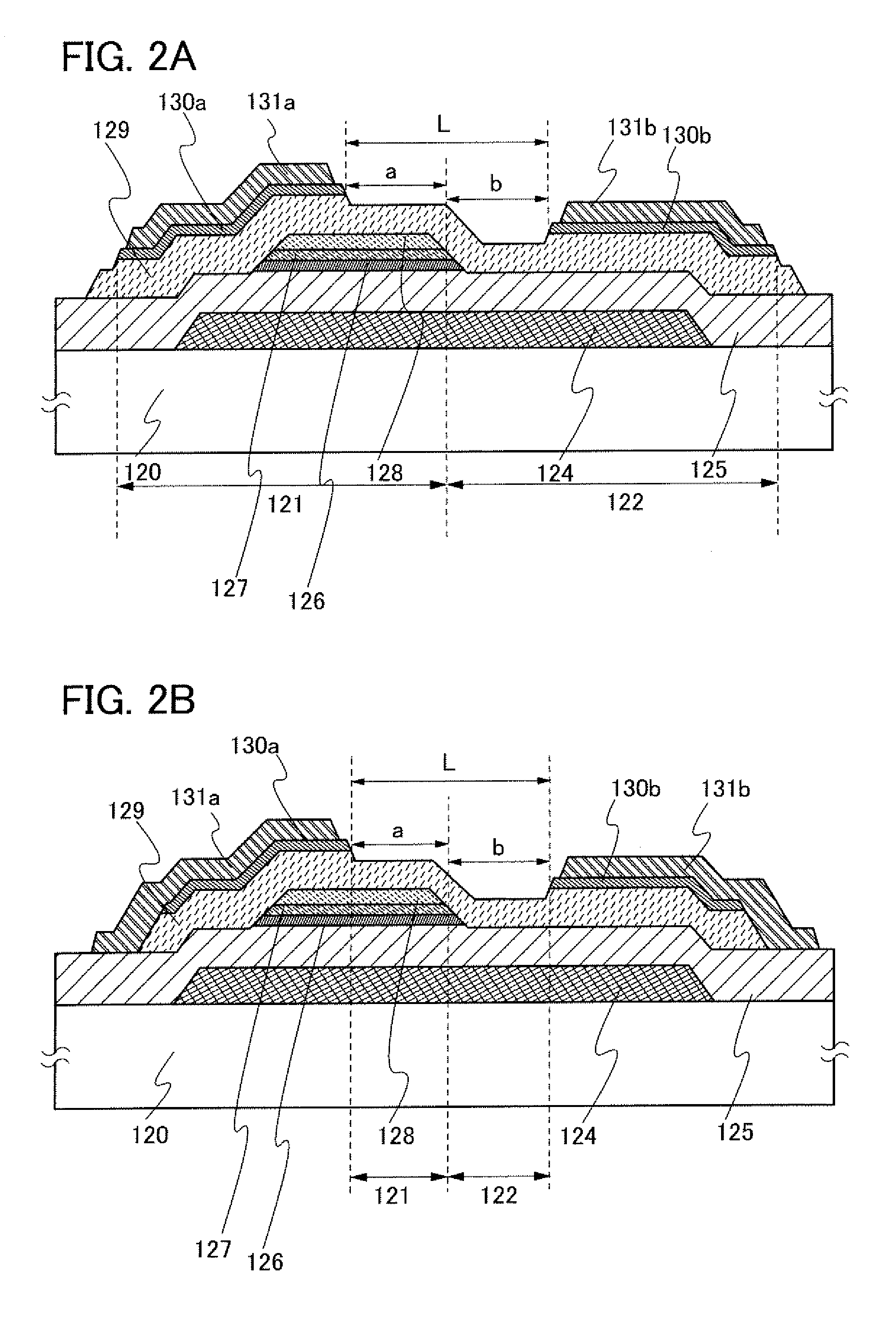
[0092]In Embodiment 2, examples of a structure of a thin film transistor according to an embodiment of the present invention, which are different from those of Embodiment 1, will be described with reference to FIGS. 2A and 2B. Note that the description about the same portions as those in Embodiment 1 will be omitted.

[0093]A thin film transistor illustrated in FIG. 2A includes a gate electrode layer 124 which is provided over a substrate 120; a first insulating layer 125 which is provided so as to cover the gate electrode layer 124; an impurity semiconductor layer 130a and an impurity semiconductor layer 130b forming a source region and a drain region, which are provided with a distance therebetween and which at least partly overlap with the gate electrode layer 124; a microcrystalline semiconductor layer 127 which is provided over the first insulating layer 125 in part of a channel formation region, and which at least partly overlaps with the gate electrode layer 124 and one of the ...

embodiment 3

[0128]In Embodiment 3, a method for manufacturing the thin film transistor described in Embodiment 1, which is the thin film transistor illustrated in FIG. 1A, will be described with reference to FIG. 3, FIGS. 4A to 4E, FIGS. 5A to 5E, and FIGS. 6A and 6B. Note that a method for manufacturing the thin film transistor illustrated in FIG. 2A is similar to that of the thin film transistor illustrated in FIG. 1A.

[0129]An n-channel thin film transistor including an amorphous semiconductor layer or a microcrystalline semiconductor layer has higher field-effect mobility than a p-channel one and thus is more suitable for being used for a driver circuit. In addition, it is preferable that thin film transistors be manufactured to have the same polarity over the same substrate because the number of manufacturing steps is reduced. Therefore, in this embodiment, a method for manufacturing an n-channel thin film transistor will be described. Note that a p-type thin film transistor can be manufact...


PUM

PropertyMeasurementUnit
sizeaaaaaaaaaa
sizeaaaaaaaaaa
electric conductivityaaaaaaaaaa

Abstract

A thin film transistor with favorable electric characteristics is provided, which includes a gate electrode layer; a first insulating layer covering the gate electrode layer; a pair of impurity semiconductor layers forming source and drain regions, which are provided with a distance therebetween and at least partly overlap with the gate electrode layer; a microcrystalline semiconductor layer which is provided over the first insulating layer in part of a channel formation region, and at least partly overlaps with the gate electrode layer and does not overlap with at least one of the pair of impurity semiconductor layers; a second insulating layer between and in contact with the first insulating layer and the microcrystalline semiconductor layer; and an amorphous semiconductor layer over the first insulating layer, covering the second insulating layer and the microcrystalline semiconductor layer. The first insulating layer is a silicon nitride layer and the second insulating layer is a silicon oxynitride layer.

Description

BACKGROUND OF THE INVENTION[0001]1. Field of the Invention[0002]The present invention relates to a thin film transistor and a display device to which the thin film transistor is applied.[0003]2. Description of the Related Art[0004]As one kind of field-effect transistors, there is known a thin film transistor in which a semiconductor layer provided over a substrate having an insulating surface is used for a channel formation region. Techniques by which amorphous silicon, microcrystalline silicon, and polycrystalline silicon are used for semiconductor layers of thin film transistors have been disclosed (see Patent Documents 1 to 5). Thin film transistors have been used for, for example, liquid crystal television devices and put into practical use as switching transistors for pixels of display screens.[Reference][Patent Document][0005][Patent Document 1] Japanese Published Patent Application No. 2001-053283[0006][Patent Document 2] Japanese Published Patent Application No. H5-129608[00...

Claims


Application Information

Patent Timeline
Patent Type & Authority Applications(United States)
IPC IPC(8): H01L29/786H01L33/00G02F1/1368H01L21/28H01L21/336H01L29/417H01L29/423H01L29/49
CPCH01L27/1214H01L29/04H01L27/1288H01L29/78696H01L29/66765
Inventor JINBO, YASUHIRO
Owner SEMICON ENERGY LAB CO LTD
Why Eureka
Try Eureka