
Touch Panel Device

a technology of touch panel and rotary keyboard, which is applied in the direction of mechanical pattern conversion, instruments, computing, etc., can solve the problems of low yield rate, and achieve the effect of simplifying the structure and manufacturing process

Inactive Publication Date: 2009-10-01
ELAN MICROELECTRONICS CORPORATION
View PDF5 Cites 121 Cited by
  • Summary
  • Abstract
  • Description
  • Claims
  • Application Information

AI Technical Summary

Benefits of technology

[0009]An object of the present invention is to provide a touch panel device having simplified structure and manufacturing process.
[0013]Compared with the prior art touch panel devices, the first electrode groups and the second electrode groups are arranged on a same side of the substrate, the insulating layer serves as an electrically isolating medium of the first electrode groups and the second electrode groups, the first electrodes are electrically connected by the bridge conductors that are arranged in a different layer with the second electrodes. As a result, the present touch panel device has simplified structure and manufacturing process. In addition, a uniform sensitivity is also obtained.

Problems solved by technology

The cross talk will interfere with detecting of touch point thereby resulting in low yield rate.

Method used


Image

  • Touch Panel Device
  • Touch Panel Device
  • Touch Panel Device

Examples


Embodiment Construction

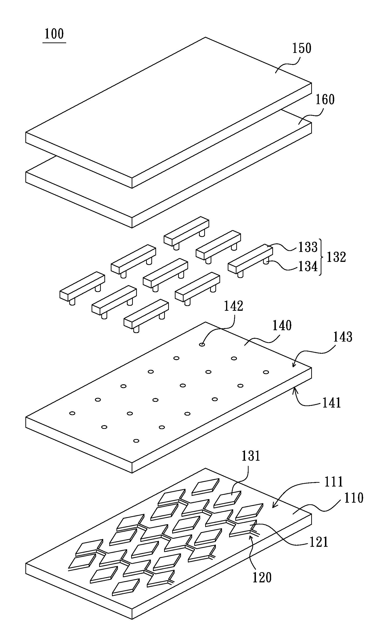
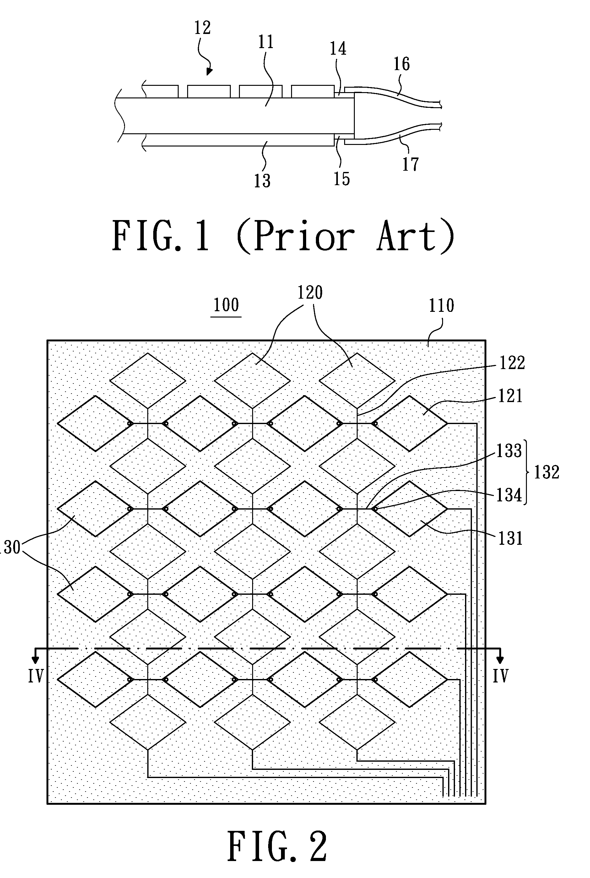
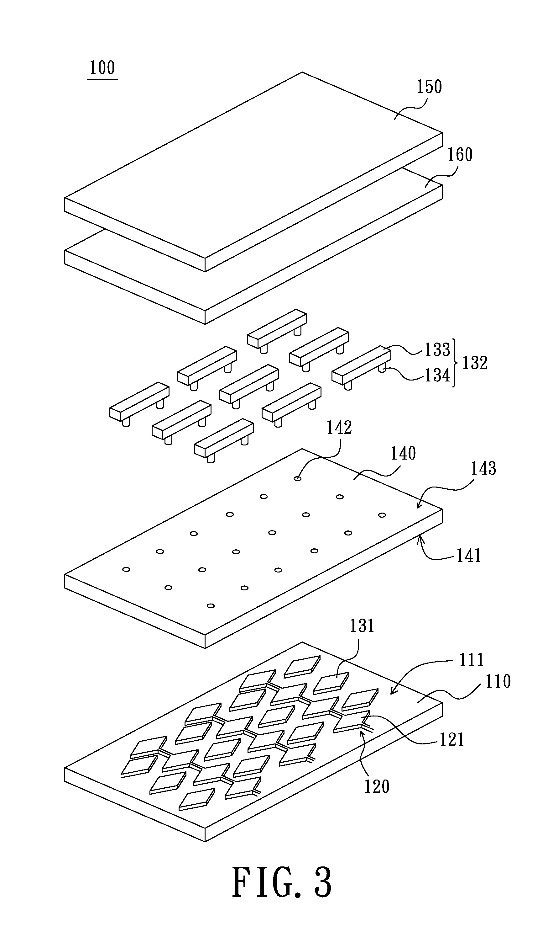
[0026]As shown in FIGS. 2 to 4, a touch panel device in accordance with a first embodiment is provided, which includes a substrate 110, a number of first electrode groups 120, a number of second electrode groups 130, an insulating layer 140, and insulating adhesive layer 160 and an anti-wearing layer 150. The substrate 110 includes a plain surface 111 for forming the first electrode groups 120 and the second electrode groups 130 thereon. The first electrode groups 120 and the second electrode groups 130 cooperatively define a capacitive sensing unit.

[0027]The first electrode groups 120 are formed on the plain surface 111 of the substrate 11. Each of the first electrode groups 120 includes a number of first electrodes 121 and a number of first leads 122. The first leads 122 lie in a same line and each electrically connects two adjacent first electrodes 121 (as shown in FIG. 2). The first electrodes 121 are spaced with / away from each other and are distributed on the plain surface of t...


PUM


Abstract

In one exemplary embodiment, a touch panel device includes a substrate, an insulating layer, a number of first electrode groups and a number of second electrode groups. The first electrode groups are formed on the first surface of the insulating layer. Each of the first electrode groups includes a number of first electrodes and a number of first leads. The first electrodes are spaced with each other. The first leads electrically connect each two adjacent first electrodes. Each of the second electrode groups includes a number of second electrodes and a number of bridge conductors electrically connecting each two adjacent second electrodes. The second electrodes are spaced with each other and are arranged on the first surface of the insulating layer. The first electrodes and the second electrodes are arranged in a staggered manner. The bridge conductors are formed on the second surface of the insulating layer.

Description

CROSS-REFERENCE TO RELATED APPLICATIONS[0001]This application is based upon and claims the benefit of priority from the prior Taiwanese Patent Application No. 097110639, filed Mar. 25, 2008, the entire contents of which are incorporated herein by reference.BACKGROUND[0002]1. Field of Invention[0003]The present invention generally relates to a touch panel device, more specifically, to a capacitive touch panel device.[0004]2. Description of Related Art[0005]Currently, touch panel devices are widely used in various kinds of electronic devices, for example, auto teller machines (ATM) of finance organizations, auto guide system in department store, personal digital assistant (PDA) or laptop computer. Touch panel devices can be sorted into several types according to different mechanisms of detecting touch point. Each type of touch panel device has different advantages and disadvantages.[0006]FIG. 1 illustrates a structure of a generally used capacitive touch panel device, which includes a...

Claims


Application Information

Patent Timeline
IPC IPC(8): G08C21/00
CPCG06F2203/04111G06F3/044G06F3/0443G06F3/0446
Inventor CHIU, YEN-CH
Owner ELAN MICROELECTRONICS CORPORATION
Learn More