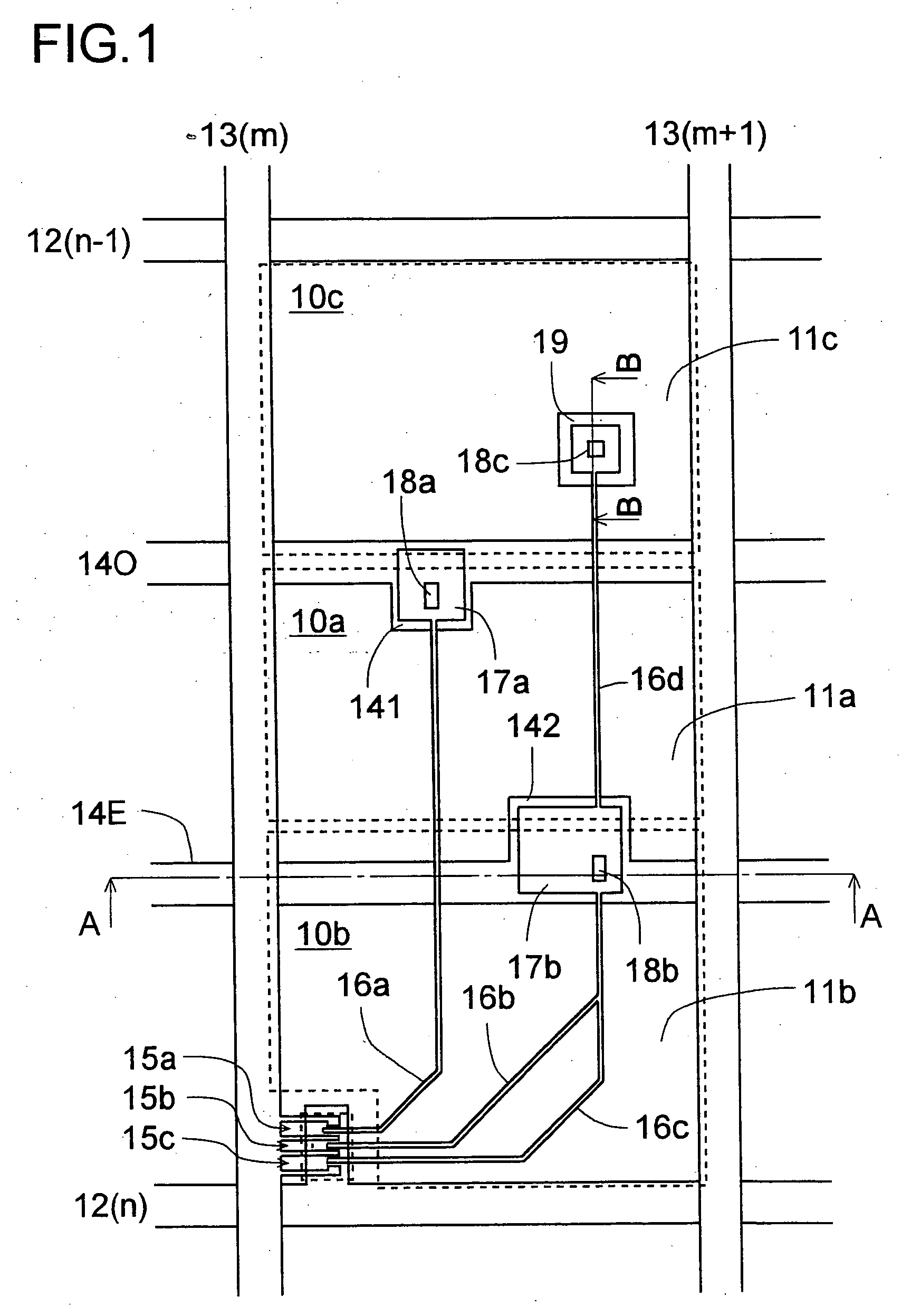
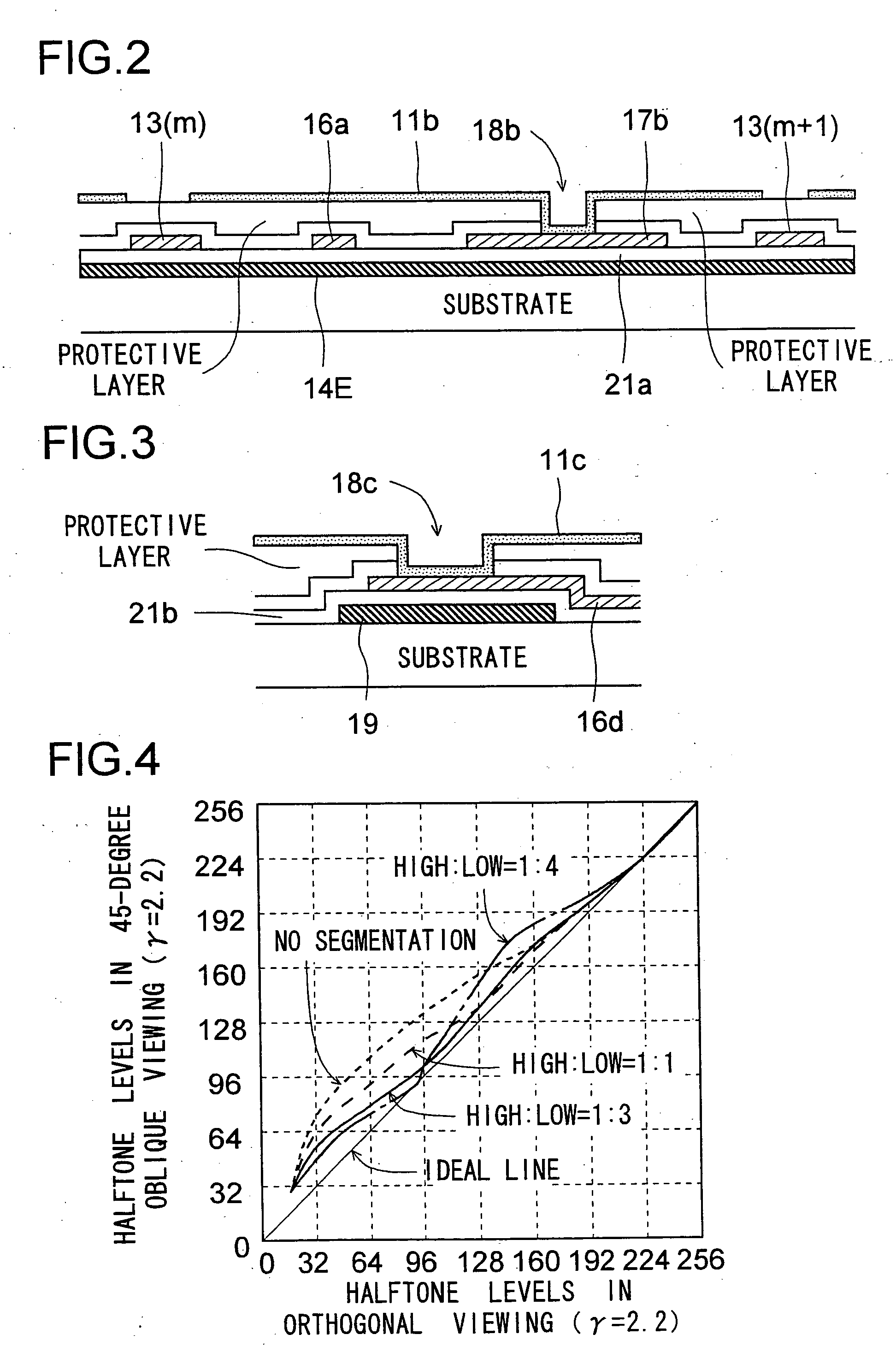
[0022]According to the present invention, in each pixel, three sub-pixels are formed that are arranged next to one another in the column or row direction. This helps further mitigate the viewing-angle dependence of the gamma characteristic as compared with that conventionally observed. Moreover, the three sub-pixels have at least two different brightness levels when the pixel as a whole is in a given middle halftone state, and the middle sub-pixel has the highest brightness level. Thus, even when an image with a straight border is displayed, the line of sight, as it moves along the border, moves across pixels having the same halftone level, unlike in a case where each pixel has two sub-pixels. This prevents the viewer from perceiving unsmoothness or unnatural hues at a border between different halftone levels.
[0023]Here, preferably, the two side sub-pixels are given an identical brightness level. This helps reduce the numbers of switching devices, auxiliary capacitance conductors, and other elements, and thus helps prevent undue lowering of the aperture ratio.
[0024]Preferably, the ratio of the aperture area of the middle sub-pixel to the total aperture area of the two side sub-pixels is in the range from 1:1 to 1:4 and, preferably, the ratio between aperture areas of the two side sub-pixels is in the range from 1:1 to 1:4. This helps further improve the gamma characteristic of the liquid crystal display.
[0025]Preferably, the three sub-pixels each have: a liquid crystal capacitance between a sub-pixel electrode and an common electrode disposed opposite each other across the liquid crystal layer; and an auxiliary capacitance between an auxiliary capacitance electrode electrically connecting to the pixel electrode and an auxiliary capacitance common electrode disposed opposite the auxiliary capacitance electrode and connecting to an auxiliary capacitance conductor; moreover, a single electrode may be shared as the common electrodes of the three sub-pixels; moreover, at least two different auxiliary capacitance conductors may provided, one for the middle sub-pixel and another for the side sub-pixels. This helps improve the controllability of the voltages applied to the sub-pixels.
[0026]Here, preferably, an insulating layer is interposed between the auxiliary capacitance electrode and the auxiliary capacitance common electrode. This allows those electrodes to overlap to form an auxiliary electrode, and thus helps increase the aperture ratio. Preferably, there are provided: scanning lines extending in the row direction; signal lines extending in the column direction; and, for each pixel, at least two switching devices that are provided one for the middle sub-pixel and another for the side sub-pixels and that connect to a scanning line and a signal line each common to the three sub-pixels of the pixel. Moreover, preferably, the switching devices are turned on and off by a scanning signal voltage supplied to the common scanning line and, when the switching devices are on, a display signal voltage is supplied from the common signal line to the sub-pixel electrode and the auxiliary capacitance electrode of each of the middle and side sub-pixels; moreover, preferably, after the switching devices are turned off, the auxiliary capacitance common voltages at the auxiliary capacitance common electrodes of the middle and side sub-pixels vary such that the variations in those voltages as defined by the directions and degrees in which they vary differ between the middle sub-pixel and the side sub-pixels. This helps further improve the controllability of the voltages applied to the sub-pixels.
[0027]Here, preferably, the switching devices are TFTs, and these TFTs are formed with a single semiconductor layer. This helps increase the aperture ratio of the pixel.
[0028]The auxiliary capacitance common voltages may invert the polarities thereof periodically; preferably, the auxiliary capacitance common voltage applied to the auxiliary capacitance common electrode of the middle sub-pixel and the auxiliary capacitance common voltage applied to the auxiliary capacitance common electrodes of the side sub-pixels are 180 degrees out of phase with each other; and, preferably, the auxiliary capacitance common voltage applied to the auxiliary capacitance common electrode of the middle sub-pixel and the auxiliary capacitance common voltage applied to the auxiliary capacitance common electrodes of the side sub-pixels have an equal amplitude. This helps further improve the controllability of the voltages applied to the sub-pixels.
[0029]Preferably, between every two mutually adjacent signal lines, display signal voltages applied thereto are given opposite polarities, in which case, preferably, between every two pixels mutually adjacent in the row direction, the auxiliary capacitance electrodes and the auxiliary capacitance common electrodes of the middle and side sub-pixels are disposed in reversed patterns. This allows the center sub-pixel to have the highest brightness.
[0030]Preferably, the scanning lines are laid between mutually adjacent pixels, and, in each pixel, the two auxiliary capacitance conductors are laid parallel to the scanning lines and between the sub-pixels. This helps improve the aperture ratio. Moreover, preferably, the conductor electrode via which the display signal voltage is supplied to the sub-pixel electrode of the middle sub-pixel is so formed as to cross the two auxiliary capacitance conductors. This helps cancel out the two parasitic capacitances formed where the conductor electrode crosses the auxiliary capacitance conductors, and thus helps improve image quality.
[0031]Preferably, a metal layer is formed under a contact hole via which the conductor electrode via which the display signal voltage is supplied connects to the sub-pixel electrode. This helps shield disturbed alignment in the liquid crystal layer, and thus helps improve image quality .


