
In-Plane Switching Mode Liquid Crystal Display Device

a liquid crystal display and switching mode technology, applied in non-linear optics, instruments, optics, etc., can solve the problem of not being able to perfectly shield static electricity, and achieve the effect of suppressing liquid crystal polarization and improving display image quality

Active Publication Date: 2009-05-14
HYDIS TECH
View PDF6 Cites 25 Cited by
  • Summary
  • Abstract
  • Description
  • Claims
  • Application Information

AI Technical Summary

Benefits of technology

[0010]Accordingly, the present invention has been made keeping in mind the above problems occurring in the related art, and an object of the present invention is to provide an in-plane switching mode liquid crystal display capable of suppressing a liquid crystal polarization due to external static electricity to improve display image quality.
[0013]The insulating layer may be over coater layer for improving planarization.

Problems solved by technology

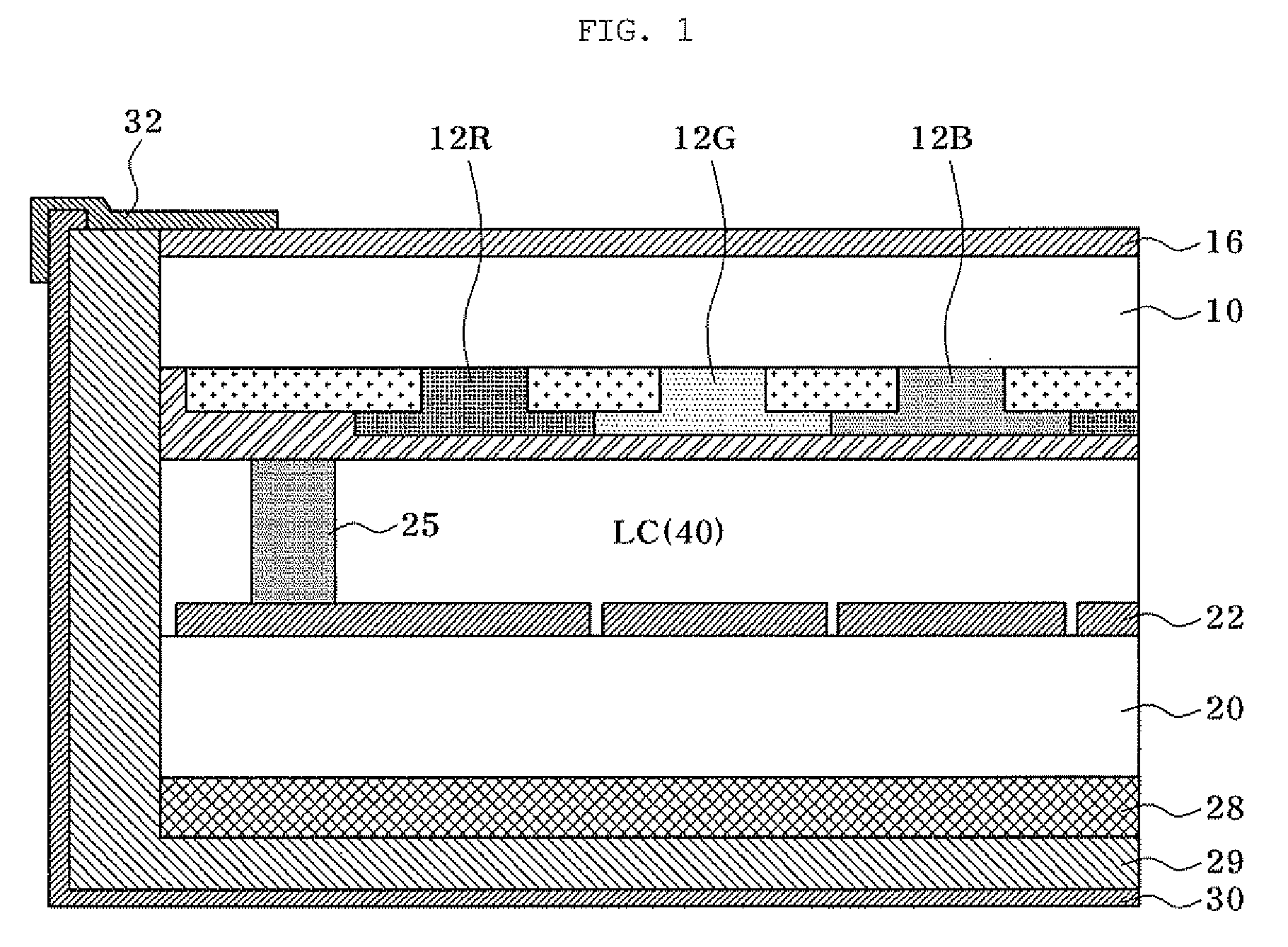
However, when the SUS bezel 30 is removed in order to form a small, lightweight and compact device such as a mobile or portable appliance, the transparent conductive layer 16 formed on the rear surface of the upper substrate 10 must be floated, making it impossible to perfectly shield the static electricity.

Method used


Image

  • In-Plane Switching Mode Liquid Crystal Display Device
  • In-Plane Switching Mode Liquid Crystal Display Device
  • In-Plane Switching Mode Liquid Crystal Display Device

Examples


Embodiment Construction

[0030]The invention is described more fully hereinafter with reference to the accompanying drawings, in which exemplary embodiments of the invention are shown. This invention may, however, be embodied in many different forms and should not be construed as limited to the exemplary embodiments set forth herein. Rather, these exemplary embodiments are provided so that this disclosure is thorough, and will fully convey the scope of the invention to those skilled in the art.

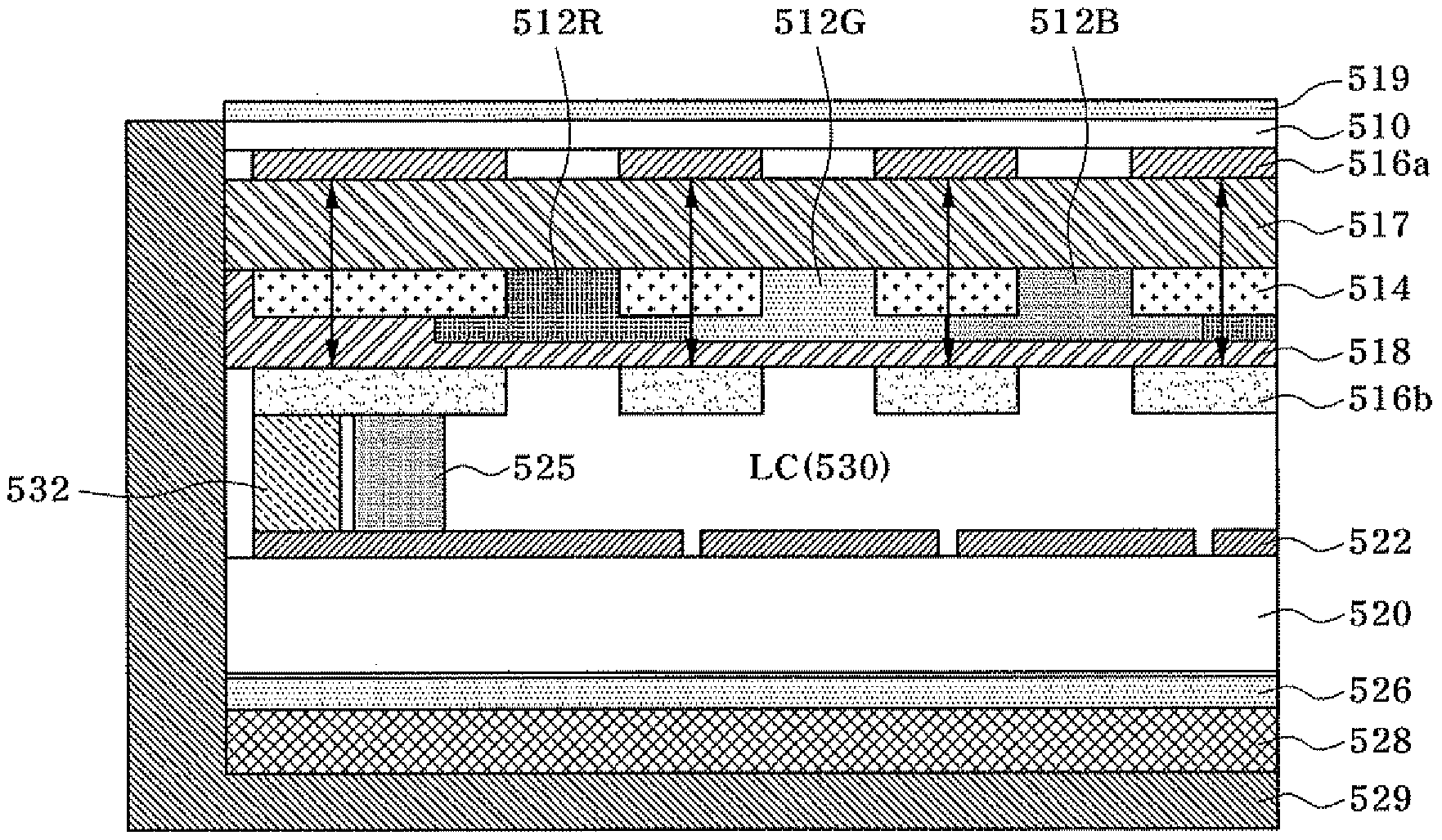
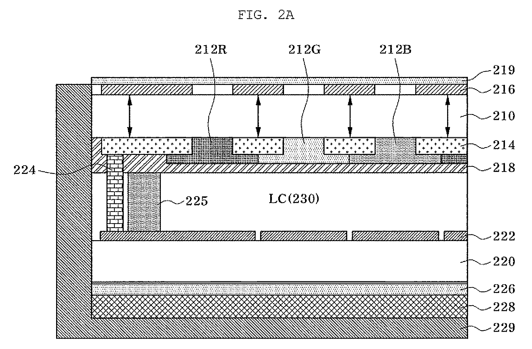
[0031]FIG. 2A is a schematic cross-sectional view of an in-plane switching mode liquid crystal display in accordance with an exemplary embodiment of the present invention, and FIG. 2B is a plan view of an in-plane switching mode liquid crystal display including a transfer dotting part of FIG. 2A.

[0032]Hereinafter, the in-plane switching mode liquid crystal display in accordance with an exemplary embodiment of the present invention will be described with reference to FIGS. 2A and 2B.

[0033]The in-plane switching mode li...


PUM

PropertyMeasurementUnit
transparentaaaaaaaaaa
conductiveaaaaaaaaaa
electric fieldaaaaaaaaaa

Abstract

Disclosed is an in-plane switching mode liquid crystal display, in which a pixel electrode and a common electrode are formed on the same substrate. The display includes a first substrate having a first conductive layer and second conductive layer, the first conductive layer and second conductive layer formed on each surface of the first substrate; a second substrate has a transparent pixel electrode and a transparent common electrode formed on one surface of the second substrate, facing the second conductive layer; an electrical connection part is installed to electrically connect the second conductive layer to the transparent common electrode, wherein a common voltage applied to the transparent common electrode is applied to the second conductive layer through the electrical connection part. This arrangement prevents generation of static electricity to suppress a whitening phenomenon due to liquid crystal polarization in a liquid crystal layer, thereby improving display image quality.

Description

BACKGROUND OF THE INVENTION[0001]1. Field of the Invention[0002]The present invention relates, in general, to an in-plane switching mode liquid crystal display device having a pixel electrode and a common electrode formed on the same substrate, and more particularly, to an in-plane switching mode liquid crystal display device capable of suppressing a liquid crystal polarization due to external static electricity to improve display image quality, by forming an induced electric field between a first conductive layer and a second conductive layer, to which a common voltage is applied through an electrical connection.[0003]2. Description of the Related Art[0004]In recent times, research on an in-plane switching mode (IPS) liquid crystal display (LCD) has been widely performed. The IPS LCD includes two electrodes formed on the same substrate such that a voltage is applied between the two electrodes to generate a horizontal electric field or a fringe electric field with respect to the sub...

Claims


Application Information

Patent Timeline
Patent Type & Authority Applications(United States)
IPC IPC(8): G02F1/1335
CPCG02F1/133512G02F2001/133334G02F1/134363G02F1/0136G02F1/133514G02F2001/134318G02F1/133334G02F1/134318G02F1/133528G02F1/13439
Inventor LIM, DONG HOON
Owner HYDIS TECH
Learn More