Semiconductor device and method for manufacturing the same

a technology of semiconductors and semiconductors, applied in the field of semiconductor devices, can solve the problems of reducing the size of the device and the inability of the current memory structure to overcome the problem, and achieve the effect of small size and good and reliable operation property

Active Publication Date: 2009-04-23
MACRONIX INT CO LTD
View PDF11 Cites 13 Cited by
  • Summary
  • Abstract
  • Description
  • Claims
  • Application Information

AI Technical Summary

Benefits of technology

[0007]The invention is directed to a semiconductor device and a method for manufacturing the semiconductor device having a gate all around structure, wherein only one single channel structure exists between a source and a drain of the semiconductor device so that the semiconductor device with the small size may possess the good and reliable operation property.

Problems solved by technology

With the further reduction of the device size, however, the current memory structure still cannot overcome the problem of the caused physical limitation.
For example, the control of the gate for switching the channel current encounters a bottleneck.

Method used


Image

  • Semiconductor device and method for manufacturing the same
  • Semiconductor device and method for manufacturing the same
  • Semiconductor device and method for manufacturing the same

Examples


Embodiment Construction

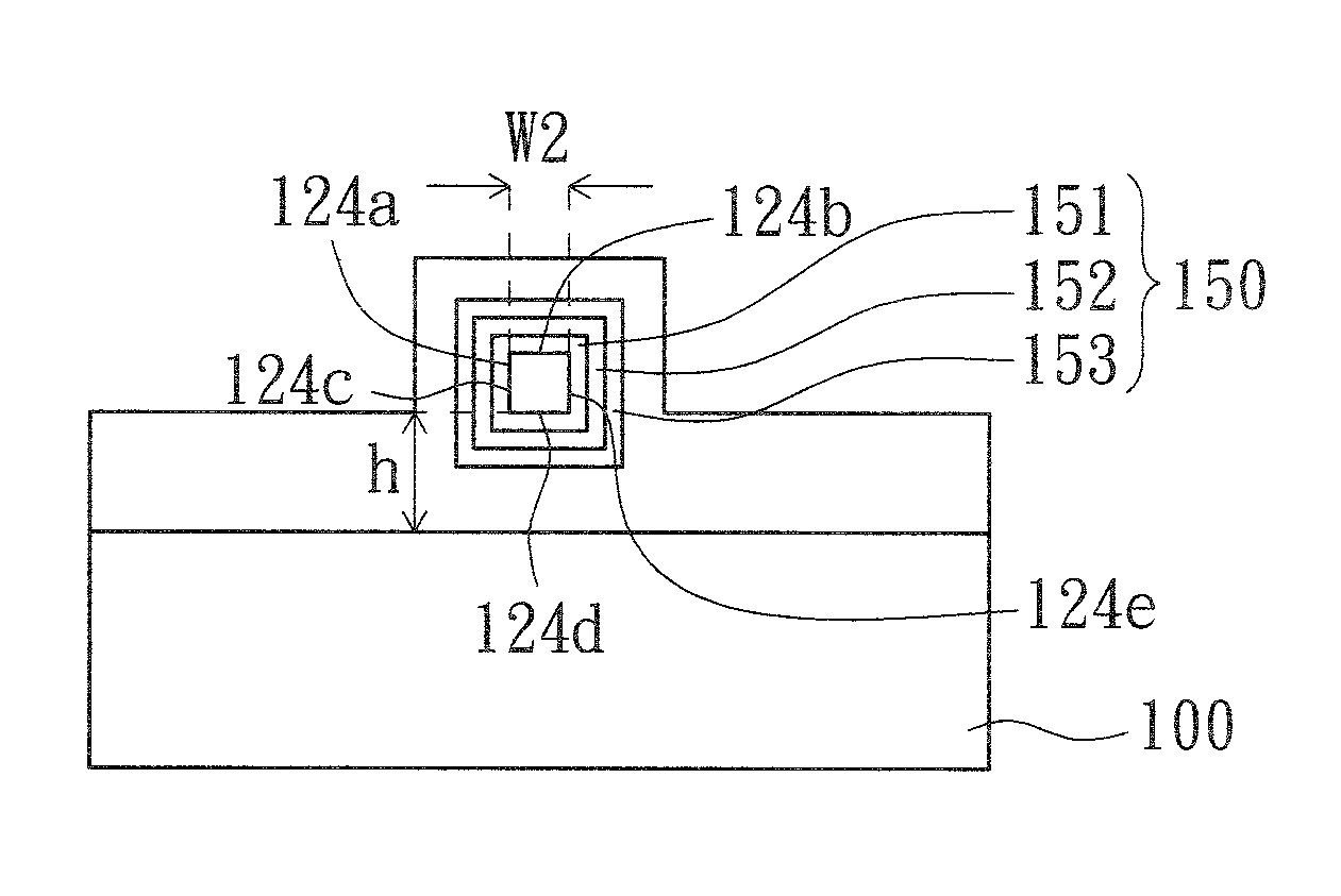
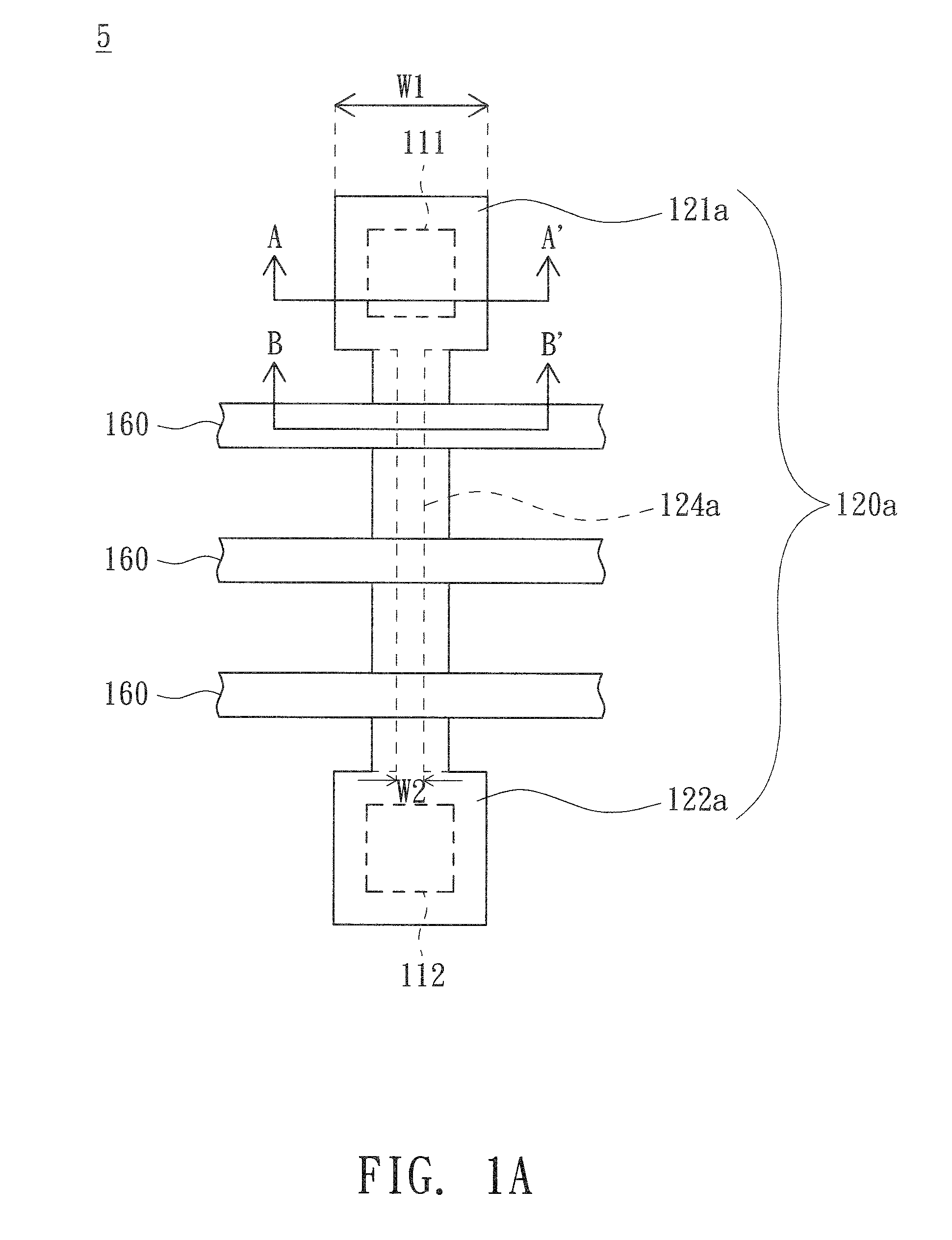
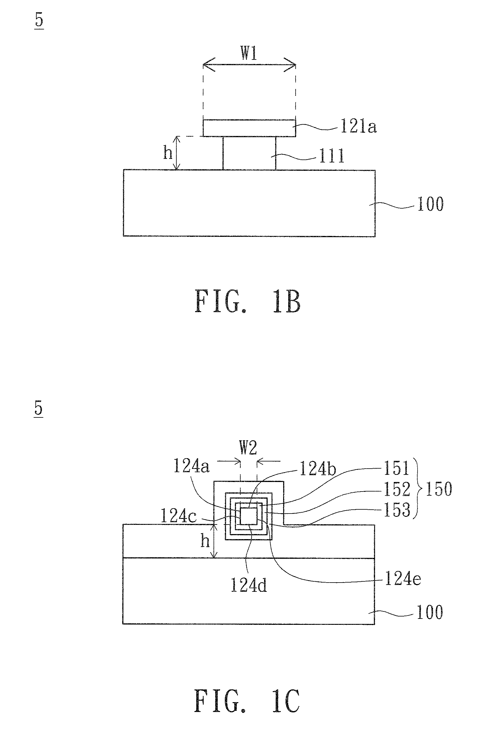
[0039]FIG. 1A is a top view showing a semiconductor device according to a preferred embodiment of the invention, and FIGS. 1B and 1C are cross-sectional views taken along lines AA′ and BB′ of FIG. 1A. Referring to FIGS. 1A to 1C, the semiconductor device 5 includes an insulating layer 100, two supporting pillars 111 and 112, a channel structure 120a, an insulating structure 150 and gates 160. The two supporting pillars 111 and 112 protrude from the insulating layer 100. The channel structure 120a includes two platforms 121a and 122a and a channel bridge 124a. The two platforms 121a and 122a are respectively disposed on the two supporting pillars 111 and 112 and are separated from the insulating layer 100 by a distance h. The channel bridge 124a connects the platforms 121a and 122a together. A bottom of the channel bridge 124a is separated from the insulating layer 100 by the distance h. The insulating structure 150 wraps around the channel bridge 124a, and the gates 160 wrap around ...


PUM


Abstract

A semiconductor device includes an insulating layer, a channel structure, an insulating structure and a gate. The channel structure includes a channel bridge for connecting two platforms. The bottom of the channel bridge is separated from the insulating layer by a distance, and the channel bridge has a plurality of separated doping regions. The insulating structure wraps around the channel bridge, and the gate wraps around the insulating structure.

Description

[0001]The application claims the benefit of U.S. Provisional Application No. 60 / 980,798, filed on Oct. 18, 2007. The subject matter of which is incorporated herein by reference.BACKGROUND OF THE INVENTION[0002]1. Field of the Invention[0003]The invention relates in general to a semiconductor device and a method for manufacturing the same, and more particularly to a semiconductor device having a gate all around (GAA) structure and a method for manufacturing the same.[0004]2. Description of the Related Art[0005]Various novel semiconductor structures have been proposed with the progress of the semiconductor manufacturing technology, by which the device size is gradually reduced, in order to solve the problem of the physical limitation accompanying therewith. Taking a memory structure as an example, an equivalent width of a channel is increased using a three-dimensional structure. A fin gate memory including a double gate structure or a tri-gate structure is an example of novel memory s...

Claims


Application Information

Patent Timeline
Patent Type & Authority Applications(United States)
IPC IPC(8): H01L29/792H01L21/336
CPCH01L21/8221H01L29/0673H01L27/0688H01L27/11568H01L27/11578H01L27/1203H01L29/42392H01L29/66787H01L29/66833H01L29/78696H01L29/792B82Y10/00B82Y40/00H01L29/66439H01L29/775H01L21/84H10B43/30H10B43/20
Inventor LAI, ERH-KUNLUE, HANG-TING
Owner MACRONIX INT CO LTD
Why Eureka
Try Eureka