Semiconductor device
a technology of semiconductor devices and semiconductors, applied in the direction of semiconductor devices, electrical apparatus, transistors, etc., can solve the problems of difficult to achieve high withstand voltage and difficult to improve the integration degree of electric power semiconductor devices, so as to improve the high withstand voltage performance and reduce the concentration of electric fields
- Summary
- Abstract
- Description
- Claims
- Application Information
AI Technical Summary
Benefits of technology
Problems solved by technology
Method used
Image

Examples
first embodiment
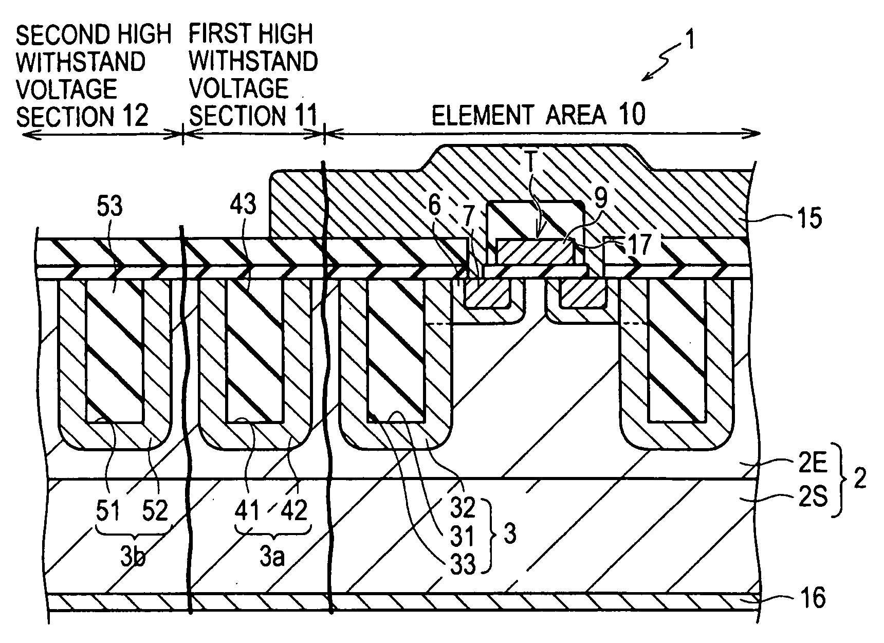
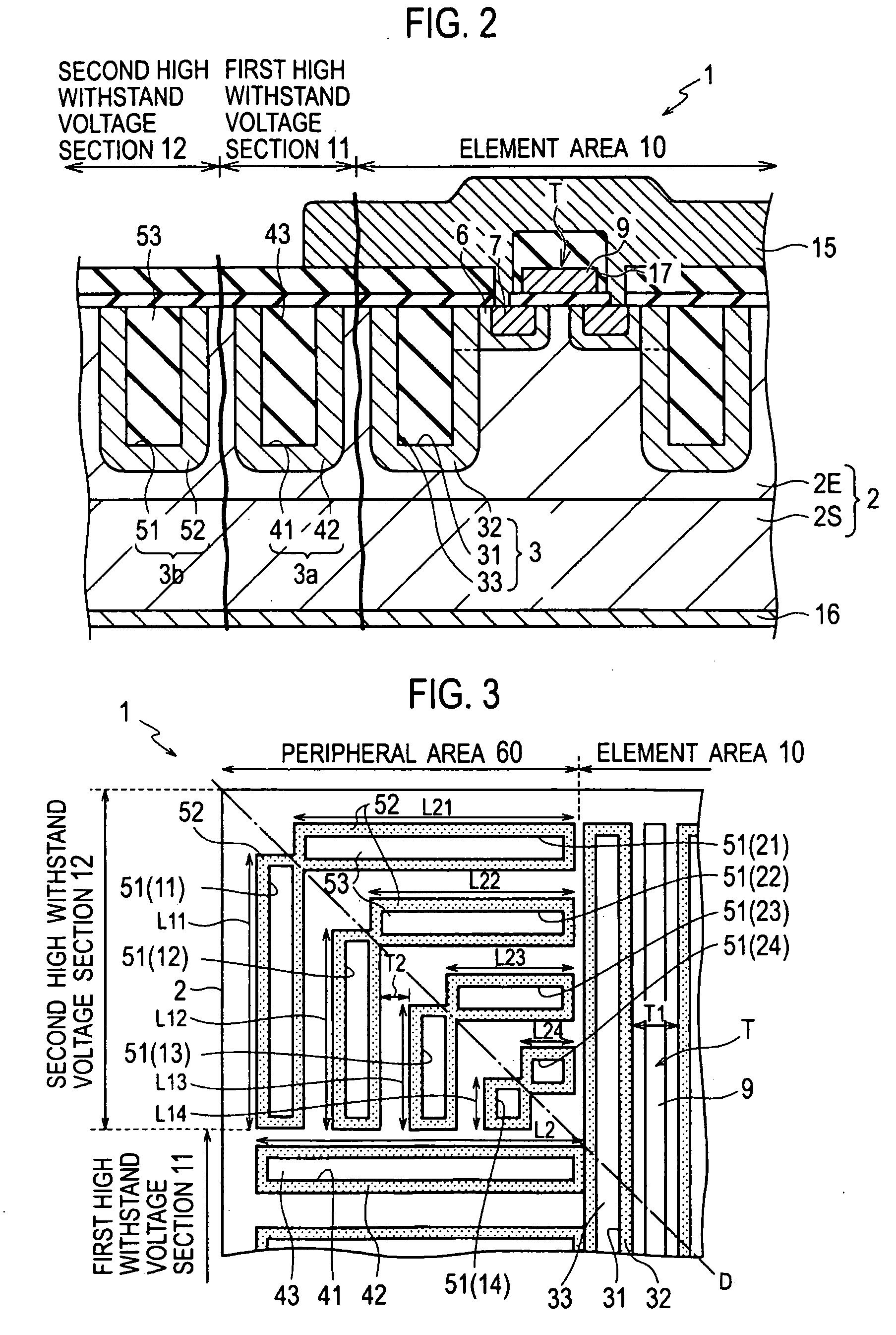
[0032]A first embodiment of the invention relates to an electric power semiconductor device including a vertical power transistor.
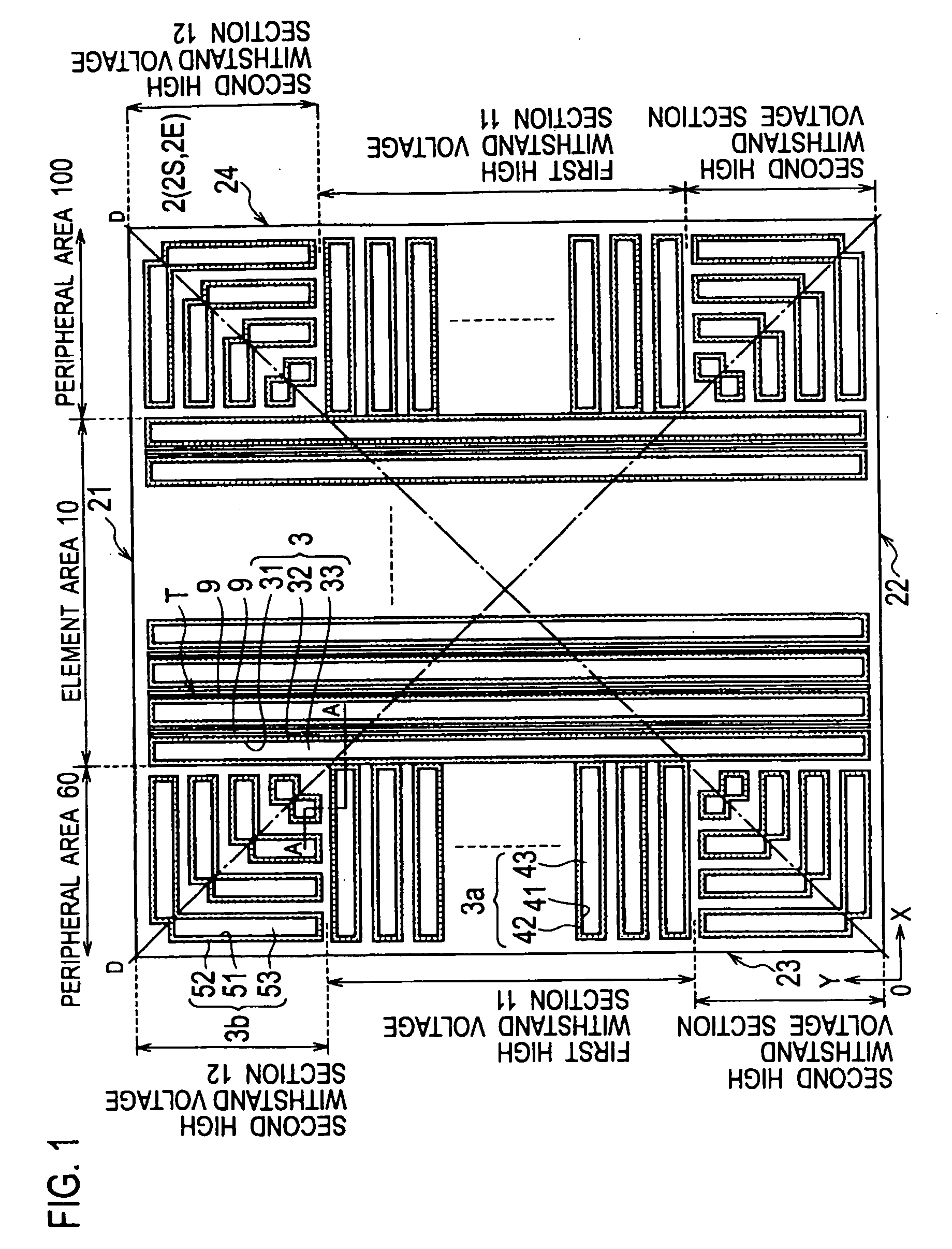
[0033]Referring to FIG. 1 and FIG. 2, a semiconductor device 1 includes: a planar rectangular substrate 2; a plurality of first RESURF structures 3 being in the shape of flat stripes, positioned at the central area of a main surface of the substrate 2 and having a long side extending in a direction (Y-direction) between a first side 21 (shown at an upper part in FIG. 1) and a second side 22 (shown at a lower part in FIG. 1) of the substrate 2 and in a direction (X-direction) between a third side 23 (shown at a left part in FIG. 1) adjacent to the first side 21 and a fourth side 24 (shown at a right part in FIG. 1), the first side 21 and the second 22 facing with each other, and the third side 23 and the fourth side 24 facing with each other; a transistor T, for instance, between the first RESURF structures 3 at the central area of the substrate 2; a first...
second embodiment
[0050]In a second embodiment of the invention, a semiconductor device 1 includes a second high withstand voltage section 12 whose RESURF layer has a shape different from the planar shape of the second high withstand voltage section 12 of the first embodiment.
[0051]Referring to FIG. 5, the second high withstand voltage section 12 of this embodiment includes second trenches 51 in the shape of a square. The p type semiconductor regions (RESURF layers) 52 are provided on the n type semiconductor region 2E and along the second trenches 51. The insulant 53 is filled in the second trenches 51. Similarly to the second high withstand voltage section 12 of the first embodiment, the second trenches 51 and the p type semiconductor regions 52 are symmetrically arranged with respect to the diagonal line D. In other words, the RESURF layers are freckled on the second high withstand voltage section 12. With the high withstand voltage section 12, the length L1 in the first direction is equal to the ...
third embodiment
[0055]In a third embodiment, the second high withstand voltage section 12 has a RESURF structure of which arrangement is somewhat different from the RESURF structure in the first or second embodiment.
[0056]Referring to FIG. 6, spaces between adjacent second trenches 51 or p type semiconductor regions 51 gradually become large toward the central area of the substrate 2 from the corner of the substrate 2. In other words, the spaces T21, T22 and T23 between the adjacent second trenches 51 and the p type semiconductor regions 52 (RESURF layers) are defined to be:
PUM
 Abstract
Description
Claims
Application Information
 - R&D
- Intellectual Property
- Life Sciences
- Materials
- Tech Scout
- Unparalleled Data Quality
- Higher Quality Content
- 60% Fewer Hallucinations
Browse by: Latest US Patents, China's latest patents, Technical Efficacy Thesaurus, Application Domain, Technology Topic, Popular Technical Reports.
© 2025 PatSnap. All rights reserved.Legal|Privacy policy|Modern Slavery Act Transparency Statement|Sitemap|About US| Contact US: help@patsnap.com