Vertical light emiting diode and method of making a vertical light emiting diode

a technology of vertical light and diodes, which is applied in the direction of semiconductor/solid-state device manufacturing, electrical equipment, semiconductor devices, etc., can solve the problems of difficult to differentiate the interface between the different layers, insufficient led, inefficient led,

Active Publication Date: 2009-02-12
HONG KONG APPLIED SCI & TECH RES INST
View PDF6 Cites 20 Cited by
  • Summary
  • Abstract
  • Description
  • Claims
  • Application Information

AI Technical Summary

Benefits of technology

[0009]Still other embodiments of the present invention will become readily apparent to those skilled in the art from the following detailed description, wherein embodiments of the invention are described by way of illustration. As will be realized, the invention is capable of other and different embodiments and its several details are capable of modifications in various respects, all without departing from the spirit and the scope of the present invention.

Problems solved by technology

However, the known methods of manufacturing vertical GaN-based LEDs have limitations in that the LLO process can be inadequate and inefficient for manufacturing reliable, efficient LED.
Also, due to the similar etching selectively of the various GaN layers, it can be difficult to differentiate the interface between the different layers.

Method used


Image

  • Vertical light emiting diode and method of making a vertical light emiting diode
  • Vertical light emiting diode and method of making a vertical light emiting diode
  • Vertical light emiting diode and method of making a vertical light emiting diode

Examples


Embodiment Construction

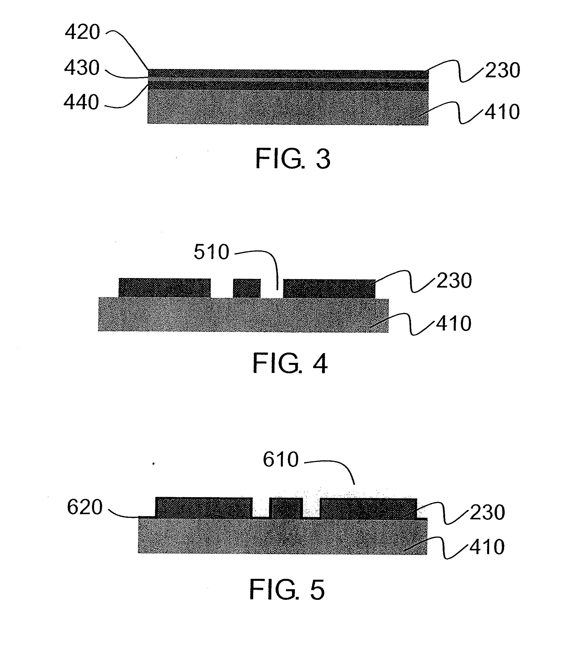
[0036]In the following description, reference is made to the accompanying drawings where, by way of illustration, specific embodiments of the invention are shown. It is to be understood that other embodiments may be used as structural and other changes may be made without departing from the scope of the present invention. Also, the various embodiments and aspects from each of the various embodiments may be used in any suitable combinations. Accordingly, the drawings and detailed description are to be regarded as illustrative in nature and not as restrictive.

[0037]Generally, the present invention is directed to a vertical GaN-based LED and to a method of making a vertical GaN-based LED. In one embodiment, the vertical GaN-based LED is made using a stop layer. FIGS. 3 to 11B are directed generally to a mechanical thinning method, such as grinding, lapping, polishing, and / or chemical mechanical polishing, used in a semiconductor fabrication process, such as the manufacture of LED, usin...


PUM


Abstract

A vertical gallium-nitrate-based LED and method of making a vertical gallium-nitrate-based LED using a stop layer is provided. Embodiments of the present invention use mechanical thinning and a plurality of superhard stop points to remove epitaxial layers with a high level of certainty. According one embodiment, the method of making a vertical LED includes forming a plurality of layers on a sapphire substrate, forming a plurality of stop points in the plurality of layers, removing the sapphire substrate and part of a u-GaN layer using mechanical thinning, wherein the mechanical thinning stops at an end of the plurality of stop points, selectively etching the u-GaN layer and exposing at least a part of the highly doped stop layer, and forming an n-electrode on the highly doped stop layer.

Description

CROSS-REFERENCE TO RELATED APPLICATIONS[0001]This application is a continuation-in-part of U.S. patent application Ser. No. 11 / 891,466, filed on Aug. 10, 2007, the disclosure of which is incorporated fully by reference.FIELD OF THE INVENTION[0002]The present invention relates to a vertical light emitting diode (LED), and more particularly, to a vertical gallium-nitride (GaN)-based LED and method of making a vertical GaN-based LED using a stop layer.BACKGROUND OF THE INVENTION[0003]Semiconductors that contain nitrogen (N) as the Group V element have proven to be useful for short-wavelength light emitting devices because of their wide band gap. Among these, extensive research has been conducted on gallium-nitride based semiconductors for use as light emitting diodes, such as AlGaInN, and such light emitting diodes (LED) have already been put to practical use.[0004]Generally, GaN-based LED are grown on a sapphire substrate. The sapphire substrate is rigid and electrically nonconductive...

Claims


Application Information

Patent Timeline
IPC IPC(8): H01L33/00H01L21/00
CPCH01L33/0079H01L33/0093
Inventor CHU, HUNG SHENCAI, YONG
Owner HONG KONG APPLIED SCI & TECH RES INST
Why Eureka
Try Eureka