Optical waveguide device and manufacturing method thereof

a technology of optical waveguides and manufacturing methods, applied in the direction of optical waveguide light guides, optical elements, instruments, etc., can solve the problems of affecting the optical path, affecting the insertion of adhesives, etc., and achieve the effect of accurately and easily forming the reflection surface in position, and easy positioning

Inactive Publication Date: 2009-01-29
NITTO DENKO CORP
View PDF8 Cites 10 Cited by
  • Summary
  • Abstract
  • Description
  • Claims
  • Application Information

AI Technical Summary

Benefits of technology

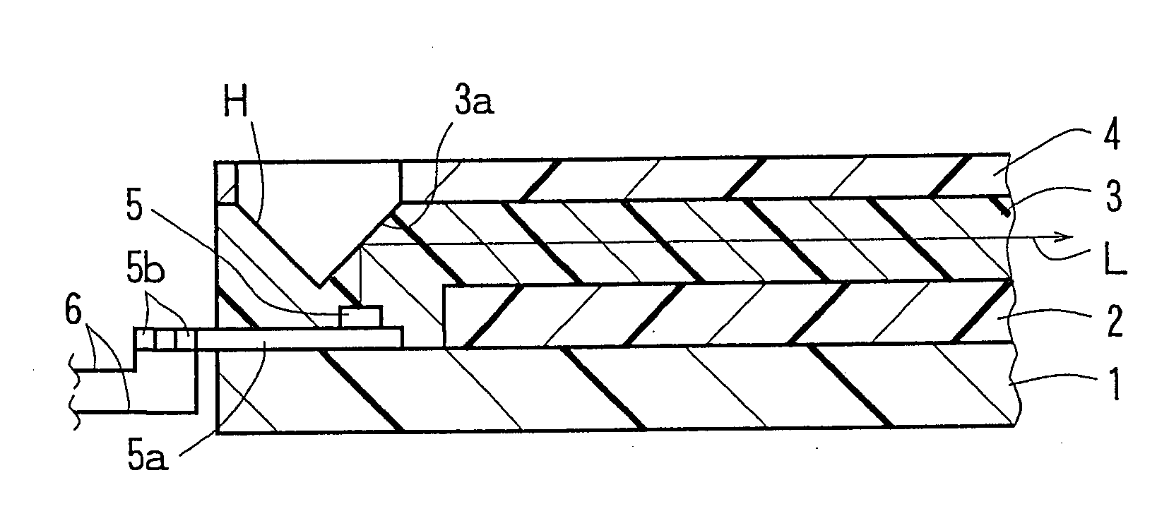
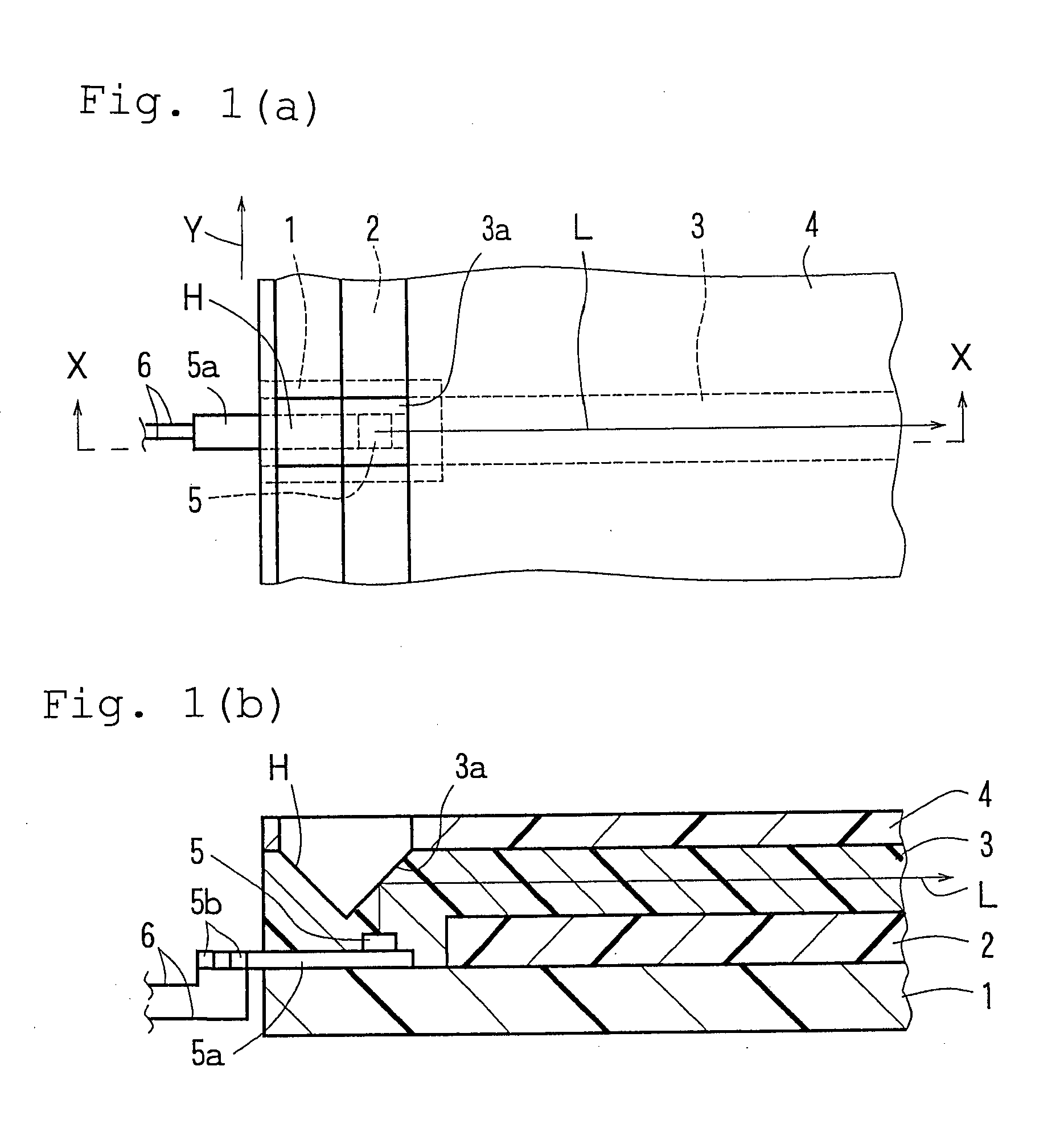
[0011]In the inventive optical waveguide device, the light emitting element and the under-cladding layer are separately provided on the upper surface of the substrate, and the core covers the light emitting element and the under-cladding layer on the substrate. Therefore, the light emitting element is held and fixed between the substrate and the core. This obviates the use of an adhesive for the fixing of the light emitting element, or eliminates the possibility of protrusion of the adhesive from the periphery of the light emitting element if a very small amount of the adhesive is used for tentatively fixing the light emitting element on the upper surface of the substrate prior to the formation of the core. The inventive optical waveguide device ensures proper light transmission between the light emitting element and the core without the possibility that the adhesive interferes with the optical path. Further, the light emitted from the light emitting element is directly inputted to the core, so that the light is more reliably inputted and transmitted as compared with the related art in which the light is inputted to the core from the light emitting element spaced from the one end face of the core.
[0012]Particularly, a reflection surface may be provided in a portion of the core associated with the light emitting element for deflecting the light emitted from the light emitting element along the light path. In this case, the light emitted from the light emitting element is reflected on the reflection surface, whereby the light is efficiently deflected along the light path in the core. Thus, the light transmission efficiency is improved.
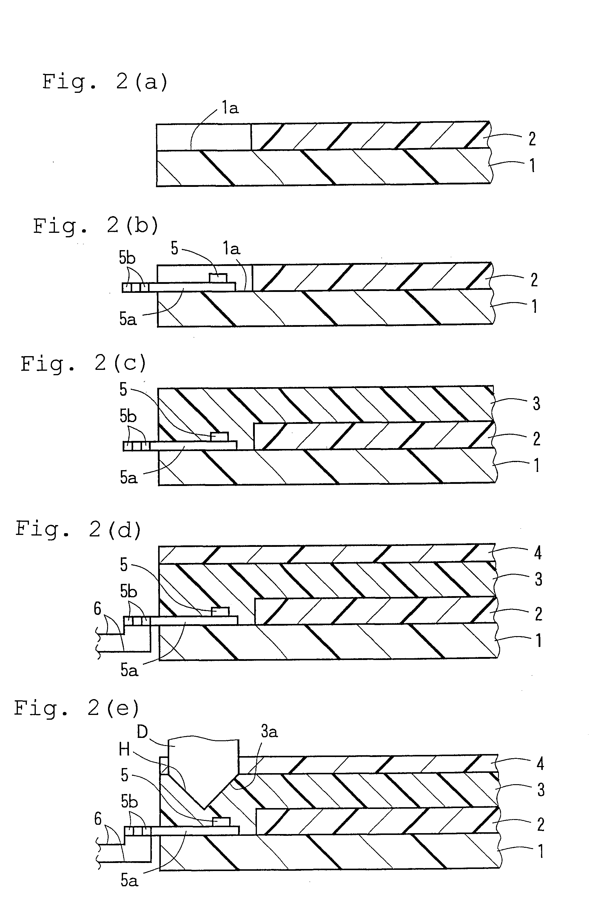
[0014]In the inventive optical waveguide device manufacturing method, the under-cladding layer is formed on the portion of the upper surface of the substrate except for the light emitting element provision region, and then the light emitting element is placed on the light emitting element provision region. Thereafter, the core is formed on the resultant substrate to cover the light emitting element and the under-cladding layer. Thus, the inventive optical waveguide device is provided, which ensures proper light transmission between the light emitting element and the core, and highly reliable light input and light transmission.
[0015]Particularly, the method may further comprise the step of forming a reflection surface in a portion of the core associated with the light emitting element, the reflection surface serving to deflect the light emitted from the light emitting element along the light path. In this case, the light emitted from the light emitting element is reflected on the reflection surface, whereby the light is efficiently deflected along the light path in the core. Thus, the optical waveguide device is provided as having an improved light transmission efficiency.
[0017]Further, the recess forming step may include the step of cutting a part of the core along a light projection axis of the light emitting element. In this case, a blade to be used for the cutting can be easily positioned. This makes it possible to accurately and easily form the reflection surface in position.

Problems solved by technology

In the optical waveguide device, however, the adhesive A is liable to protrude to interfere with an optical path when the light emitting element 50 is pressed from the above for bonding thereof.

Method used


Image

  • Optical waveguide device and manufacturing method thereof
  • Optical waveguide device and manufacturing method thereof
  • Optical waveguide device and manufacturing method thereof

Examples


example

Material for Formation of Under-Cladding Layer and Over-Cladding Layer

[0043]A material for formation of an under-cladding layer and an over-cladding layer was prepared by mixing 35 parts by weight of bisphenoxyethanolfluorene diglycidyl ether (Component A), 40 parts by weight of 3′,4′-Epoxycyclohexylmethyl-3,4-Epoxycyclohexane carboxylate which is an alicyclic epoxy resin (CELLOXIDE 2021P manufactured by Daicel Chemical Industries, Ltd.) (component B), 25 parts by weight of (3′,4′-Epoxycyclohexane)methyl-3′,4′-Epoxycyclohexyl-carboxylate (CELLOXIDE 2081 manufactured by Daicel Chemical Industries, Ltd.) (component C), and 1 part by weight of a 50% propione carbonate solution of 4,4′-bis[di(β-hydroxyethoxy)phenylsulfinio]phenylsulfide bishexafluoroantimonate (photoacid generator, Component D).

Material for Formation of Core

[0044]A material for formation of a core was prepared by dissolving 70 parts by weight of the aforementioned component A, 30 parts by weight of 1,3,3-tris{4-[2-(3-ox...


PUM


Abstract

An optical waveguide device including a substrate; a light emitting element provided on a light emitting element provision region of an upper surface of the substrate; an under-cladding layer provided on a portion of the upper surface of the substrate except for the light emitting element provision region; and a core covering the light emitting element and the under-cladding layer on the substrate, and serving as a path of light emitted from the light emitting element. An optical waveguide device manufacturing method including the steps of: forming an under-cladding layer on a portion of an upper surface of a substrate except for the light emitting element provision region; placing a light emitting element on the light emitting element provision region; and forming a core on the resultant substrate to cover the light emitting element and the under-cladding layer.

Description

RELATED APPLICATIONS[0001]This application claims the benefit of U.S. Provisional Application No. 60 / 982,237, filed on Oct. 24, 2007, which is hereby incorporated by reference.BACKGROUND OF THE INVENTION[0002]1. Field of the Invention[0003]The present invention relates to an optical waveguide device which is widely used for optical communications, optical information processing and other general optics, and to a method of manufacturing the optical waveguide device.[0004]2. Description of the Related Art[0005]In general, optical waveguide devices are configured such that light emitted from a light emitting element is transmitted through an optical waveguide (see, for example, U.S. Pat. No. 5,914,709). Such an optical waveguide device is schematically illustrated in FIG. 5. In FIG. 5, the optical waveguide device includes an optical waveguide including an under-cladding layer 20, a core 30 and an over-cladding layer 40 provided on a substrate 10. A light emitting element 50 is fixed t...

Claims


Application Information

Patent Timeline
IPC IPC(8): H01L33/00H01L33/54H01L33/56H01L33/62
CPCG02B6/1221G02B6/4202G02B6/138G02B6/12G02B6/42
Inventor HIKITA, TAKAMIMUNE, KAZUNORI
Owner NITTO DENKO CORP
Why Eureka
Try Eureka