Method for manufacturing electronic device panel and structure thereof

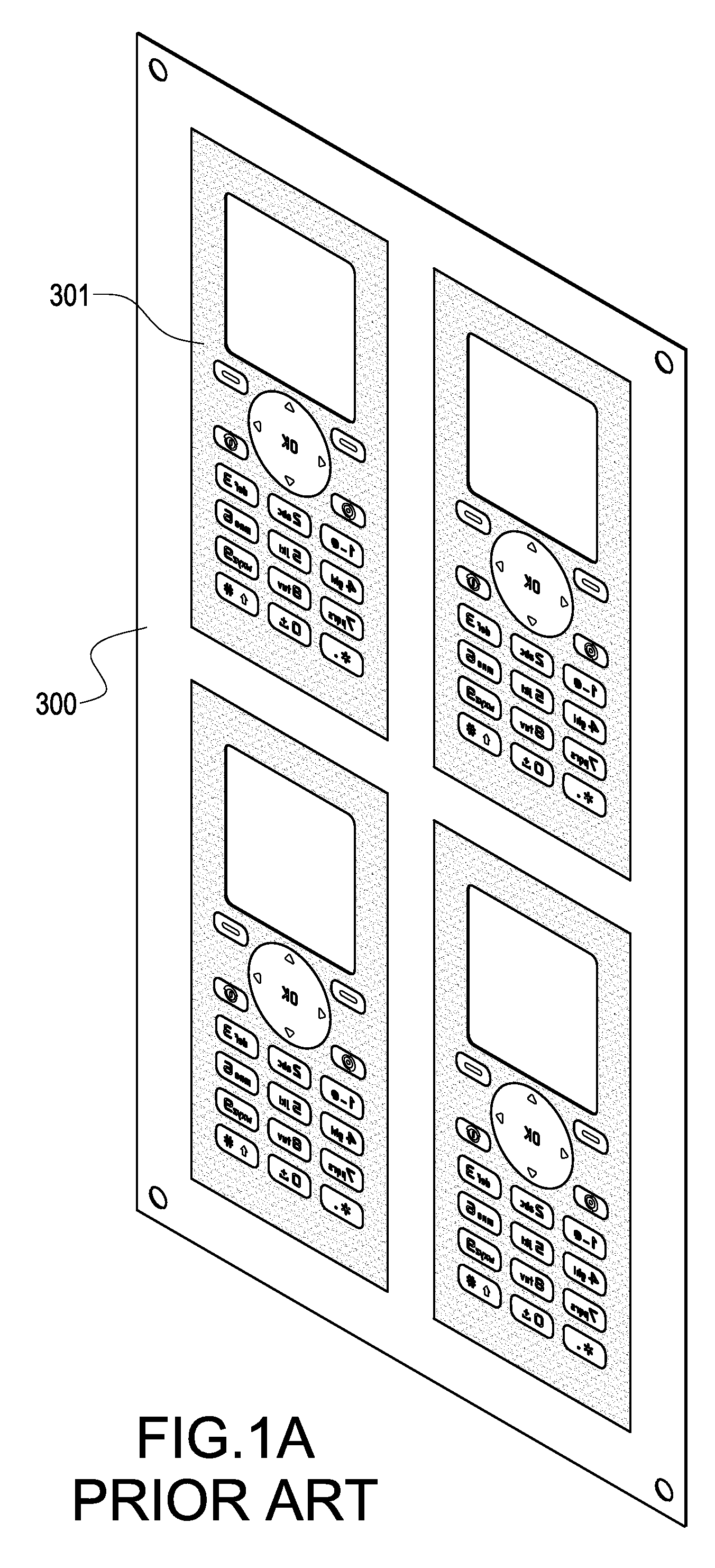
a technology of electronic devices and manufacturing methods, applied in the direction of substation equipment, interconnection arrangements, other domestic objects, etc., can solve the problems of wasting materials, and reducing the production efficiency of defective products, so as to reduce the production cost of defective products and facilitate the manufacturing of panel structures.

Inactive Publication Date: 2008-10-09
ICHIA TECH
View PDF3 Cites 16 Cited by
  • Summary
  • Abstract
  • Description
  • Claims
  • Application Information

AI Technical Summary

Benefits of technology

[0010]Therefore, the invention proposes an innovative manufacturing method for panel structure, makin...

Problems solved by technology

For example, a combination of a mobile phone and a GPS (Global Positioning System) makes a consumer possess many functions to use simultaneously, when he buys only one communication product, so that a lot of purchasing cost may be saved.
If the ink itself does not possess flexibility then, when the piece body 300 is thermally pressed into a three-dimensional panel housing 302, the bending of the three-dimensional panel housing 302 will easily make the patterns that are printed by ink gener...

Method used


Image

  • Method for manufacturing electronic device panel and structure thereof
  • Method for manufacturing electronic device panel and structure thereof
  • Method for manufacturing electronic device panel and structure thereof

Examples


Embodiment Construction

[0038]In cooperation with attached drawings, the technical contents and detailed description of the present invention will be as follows.

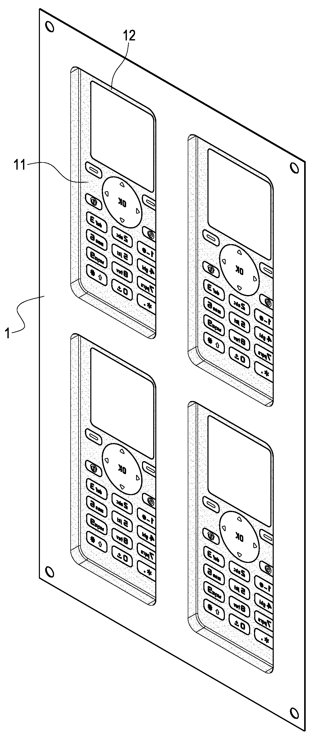
[0039]Please refer to FIG. 2 and FIG. 3, which are panel manufacturing flowchart and piece body appearance illustration of an electronic device according to the present invention. In these figures, as shown in step 100, when a panel according to the present invention is manufactured, a piece body 1 made of a material of transparent PC (polycarbonate) film is, first of all, provided.

[0040]In step 102, regarding printing process, a plurality of plane panel patterns 11 is printed on the back surface of the piece body 1 by means of ink.

[0041]In step 104, as shown in FIG. 4, the aforementioned printed panel patterns 11 are thermally pressed into three-dimensional panels projecting out of the surface of the piece body 1 under a plastically shaping process, and the printed panel patterns are located at the inside of the three-dimensional panels 12.

[0042]I...


PUM

PropertyMeasurementUnit
Electrical resistanceaaaaaaaaaa
Flexibilityaaaaaaaaaa
Transparencyaaaaaaaaaa

Abstract

A method for manufacturing a panel having a surface of three-dimensional patterns and the structure thereof, first of all, provides a piece body, on the surface of which plane panel patterns are arranged by means of ink printing process, and which is thermally pressed into a plurality of projected three-dimensional panels. The piece body having projected three-dimensional panels is then placed between a lower mould and a first upper mould. A material of hard resin is injected into the clearance between the lower mould and the three-dimensional panel surfaces, and thus a transparent cladding layer capable of wear-resistance and protection for three-dimensional panels is formed. Next, material of hard resin is again injected into the space between the inner wall surfaces of the three-dimensional panels and a second upper mould for forming a supporting layer for supporting the three-dimensional panels. Afterwards, a material of rubber is injected into the space between a third upper mould and the inner wall surfaces of three-dimensional panels to form an elastic layer. At last, castings on the piece body and three molded layers are integrally cut according to respective contour to thus complete the manufacturing process of a single panel structure.

Description

BACKGROUND OF THE INVENTION[0001]1. Field of the Invention[0002]The present invention relates to a panel structure and, in particular, to a method for manufacturing an electronic device panel consisting of a housing and a keypad.[0003]2. Description of Prior Art[0004]Following the continuous progress of technology, various communication products are successively integrated together. For example, a combination of a mobile phone and a GPS (Global Positioning System) makes a consumer possess many functions to use simultaneously, when he buys only one communication product, so that a lot of purchasing cost may be saved.[0005]However, when a general user is purchasing a mobile phone, except for the consideration of its function, he also considers other factors, such as: innovative appearance and modeling, and / or mini-size, etc. Therefore, colorful patterns or three-dimensional textures are directly arranged onto the panel of a mobile phone in current market, to induce the product's added...

Claims


Application Information

Patent Timeline
IPC IPC(8): H04M1/00
CPCB29C45/0055B29C45/1418B29C45/1671B29L2031/3437H01H13/88H01H2229/047H04M1/0283
Inventor WU, CHE-TUNG
Owner ICHIA TECH
Why Eureka
Try Eureka