
Capacitive-type touch pad having special arrangement of capacitance sensor

a capacitance sensor and capacitance sensor technology, applied in the field can solve the problems of capacitance change, control or adjustment limit the use scope of capacitive-type touch pads, such as mobile phones, and achieve the effect of reducing the capacitance chang

Inactive Publication Date: 2008-09-11
ELAN MICROELECTRONICS CORPORATION
View PDF5 Cites 29 Cited by
  • Summary
  • Abstract
  • Description
  • Claims
  • Application Information

AI Technical Summary

Benefits of technology

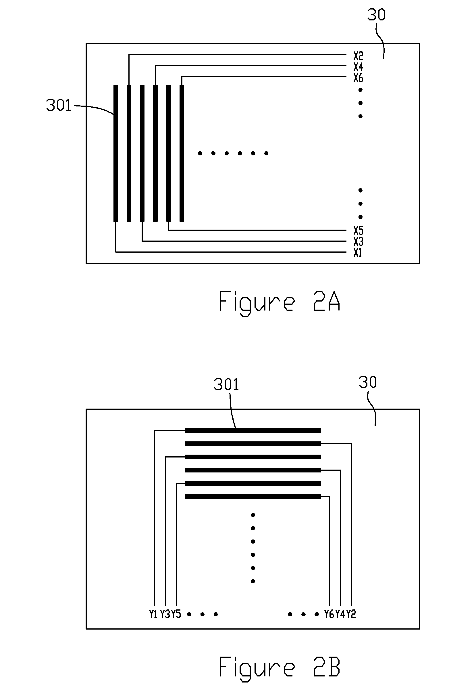
[0009]A touch pad has a controller circuitry for generating an X-Y coordinate signal; a touch screen connecting with the controller circuitry, which has a transparent substrate and a transparent conductive film provided at the transparent substrate. The transparent conductive film having a plurality of capacitance sensors distributed along an X-coordinate direction and a Y-coordinate direction. The plurality of capacitance sensors are patterned for averaging the resistance capacitance distribution.
[0011]These and other features and advantages of the various embodiments disclosed herein will be better understood with respect to the following description and drawings, in which like numbers refer to like parts throughout, and in which:

Problems solved by technology

However, generally PCB is opaque, which limit the use scope of the capacitive-type touch pads, such as mobile phone, personal Digital Assistant (PDA), display, etc.
However, ITO conductive film or IZO conductive film generally has a resistance, which can not be ignored.
Thus, the capacitance sensor far away a control circuit can not precisely detect the capacitance change, which made the control or adjustment of the capacitive-type touch pads imprecisely.
Especially, the capacitance sensor far away a control circuit can not detect the capacitance change if it is disposed under a thicker medium.

Method used


Image

  • Capacitive-type touch pad having special arrangement of capacitance sensor
  • Capacitive-type touch pad having special arrangement of capacitance sensor
  • Capacitive-type touch pad having special arrangement of capacitance sensor

Examples


Embodiment Construction

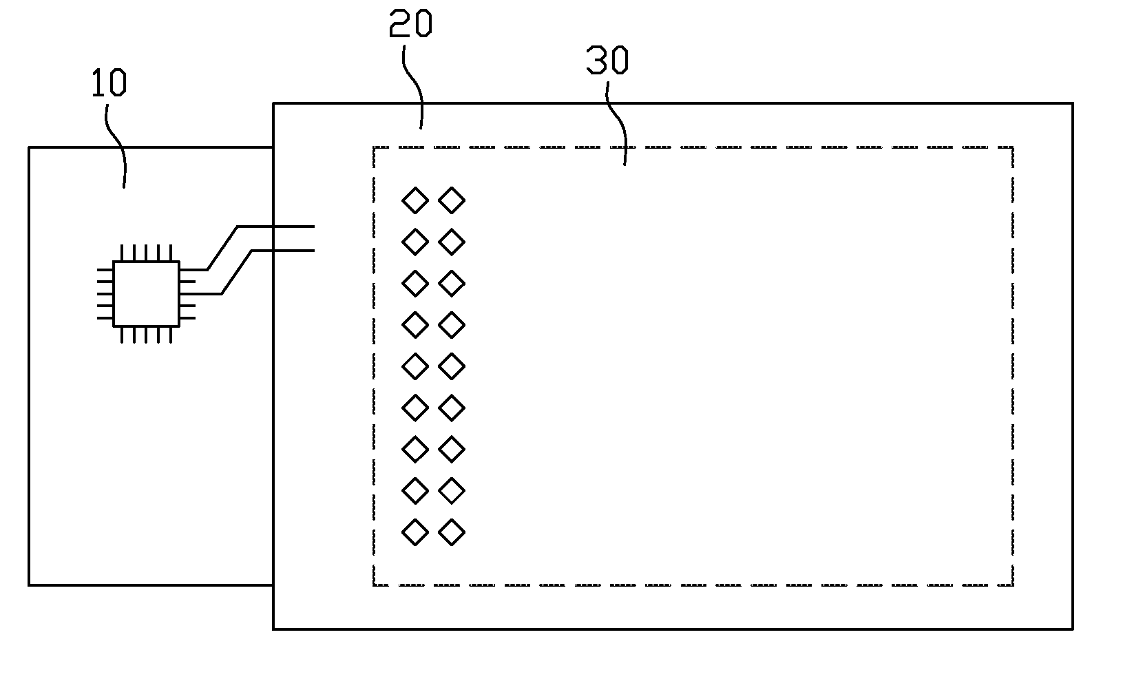
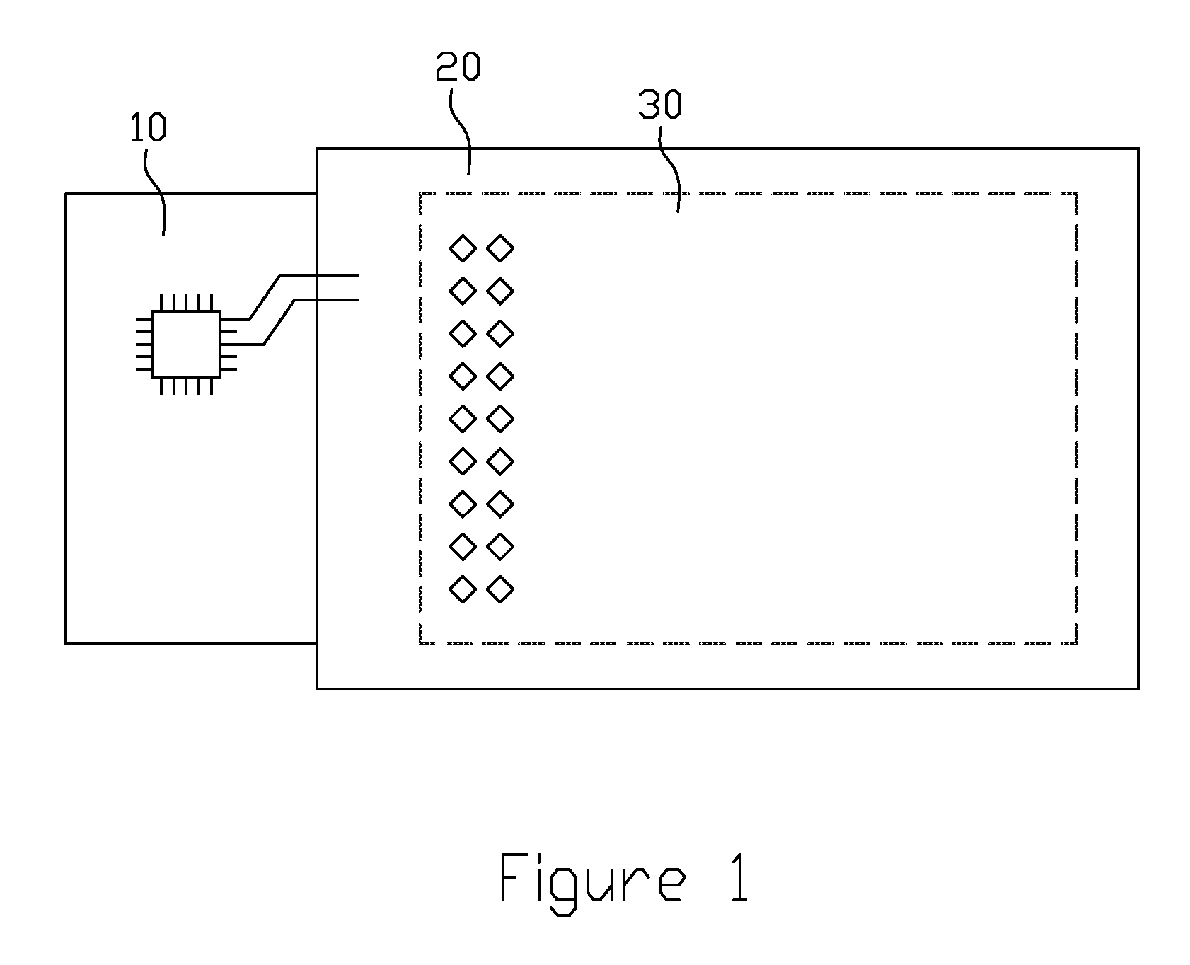
[0025]Turning now to the drawings in greater detail, there is illustrated in FIG. 1 an exemplary environment within which an embodiment, of a touch pad, screen or system in accordance with the present invention is utilized. The touch pad having a surface which is adapted to be touched by an user and which is positionable in a stationary condition across a screen of a display, which includes a flexible printed circuit board (FPCB) 10 and a touch screen 20. The FPCB 10 has a controller circuitry formed thereon, which is used to supply stimulating electrical signals to touch screen 20 and to generate an X-Y coordinate signal which corresponds with the location (i.e. the point) within the touch screen 20 at which the touch screen 20 is touched by an user. Such coordinate signals may be used by a computer to initiate a desired, i.e. a predetermined, command within the computer. The touch screen 20 has a transparent insulating substrate made of glass, on which is provided a transparent co...


PUM


Abstract

A touch pad has a controller circuitry for generating an X-Y coordinate signal; a touch screen connecting with the controller circuitry, which has a transparent substrate and a transparent conductive film provided at the transparent substrate. The transparent conductive film having a plurality of capacitance sensors distributed along an X-coordinate direction and a Y-coordinate direction. The plurality of capacitance sensors are patterned for averaging the resistance capacitance distribution.

Description

CROSS-REFERENCE[0001]This application claims priority from U.S. Provisional Patent Application No 60 / 893,623, filed on Mar. 7, 2007.BACKGROUND[0002]The present invention relates to touch pads for display devices. More particularly, the present invention relates to capacitive-type touch pads for display devices.[0003]Touch pads have been developed as a means of efficiently interfacing with electronic devices via a display surface. For example, users may input desired information using a touch pad integrated with a display device while watching images displayed by the display device. Allowing users to input desired information to an electronic device via a display surface, touch pads substantially reduce or eliminate the need for other types of input devices (e.g., keyboards, mice, remote controllers, and the like). Currently, touch pads have been widely integrated with display surfaces of flat panel display devices such as liquid crystal display (LCD) devices, plasma display panel (P...

Claims


Application Information

Patent Timeline
IPC IPC(8): G06F3/041
CPCG06F3/044G06F3/0443G06F3/0445
Inventor HUANG, CHUN-CHUNGWANG, TSUN-MINLIN, TSE-CHILIN, CHUN-YU
Owner ELAN MICROELECTRONICS CORPORATION
Learn More