
Plasma processing apparatus

a processing apparatus and plasma technology, applied in the direction of coatings, chemical vapor deposition coatings, electric discharge tubes, etc., can solve the problems of difficult selectively removing particles in the edge area, difficult to align the substrate, and deformation of the substra

Inactive Publication Date: 2008-08-28
TES CO LTD
View PDF0 Cites 324 Cited by
  • Summary
  • Abstract
  • Description
  • Claims
  • Application Information

AI Technical Summary

Benefits of technology

The present invention relates to a plasma processing apparatus that removes impurities and particles from a substrate. The technical effect of the invention is to effectively remove particles and thin films accumulated on the substrate, particularly on the edge area, without causing deformation or alignment difficulties. The invention also avoids the use of a wet etching method that causes environmental problems and increases process cost. The invention provides an apparatus for exposing and etching only the edge area of the substrate, allowing for selective removal of particles and thin films accumulated on the edge area.

Problems solved by technology

Therefore, when the process is continued without removing the particles and thin films accumulated on the substrate, the substrate may be deformed or alignment of the substrate may become difficult.
Although the wet etching is generally used to remove particles accumulated on the surface of the substrate, it is difficult to selectively remove the particles in the edge area since process management of the wet etching is difficult.
Further, the wet etching process results in an increase of the process cost by using a large amount of chemicals and causes many environmental problems such as chemical waste disposal.
However, particles accumulated between the substrate holder and the substrate are not easily removed in the above configuration.

Method used


Image

  • Plasma processing apparatus
  • Plasma processing apparatus
  • Plasma processing apparatus

Examples


Embodiment Construction

[0030]Preferred embodiments of the invention are described hereafter in detail with reference to accompanying drawings. The present invention, however, is not limited to the embodiments described herein, but may be modified in a variety of ways, and the embodiments is provided only to fully describe the invention and inform those skilled in the art of the aspects of the invention. The same reference numeral indicates the same components in the drawings.

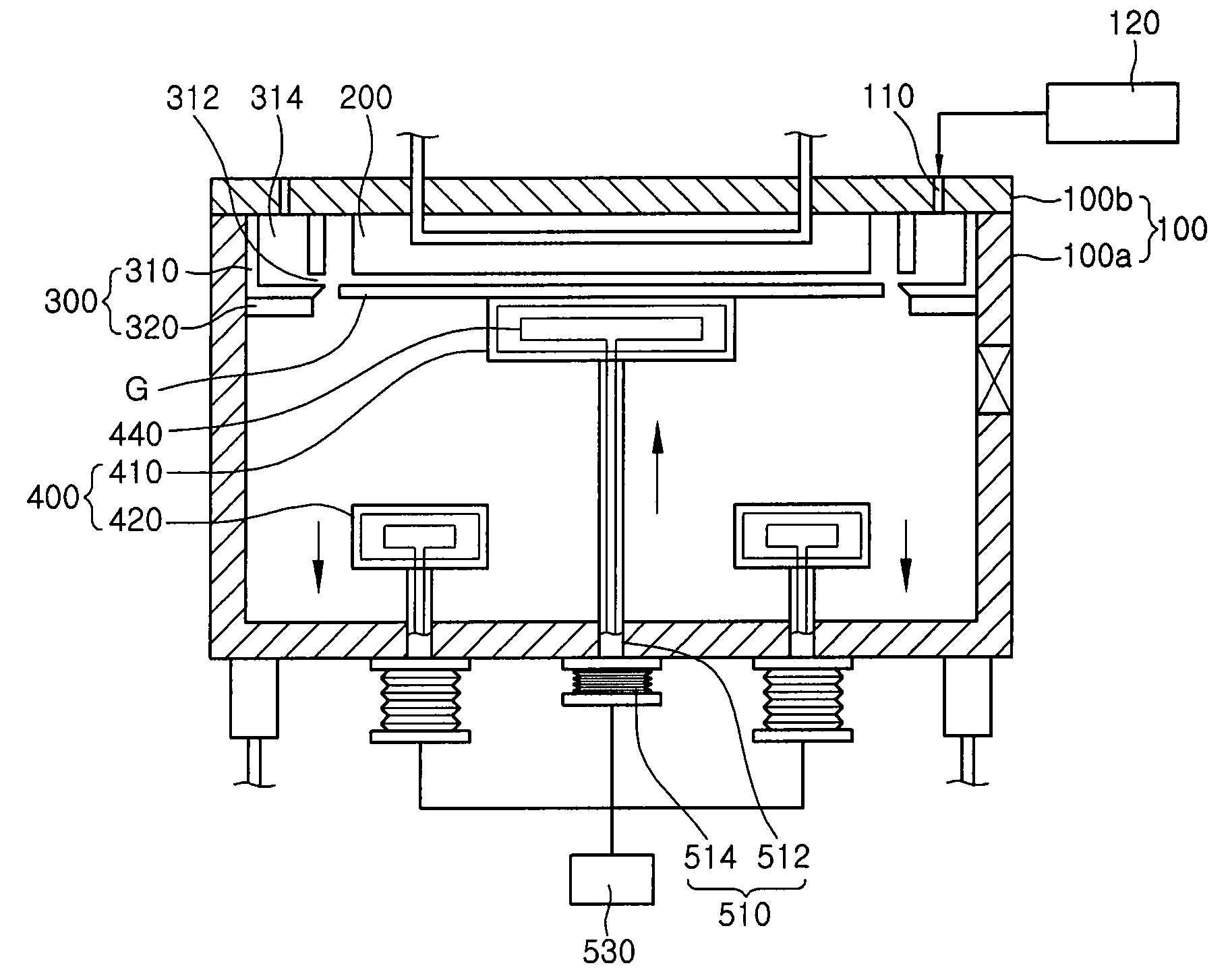
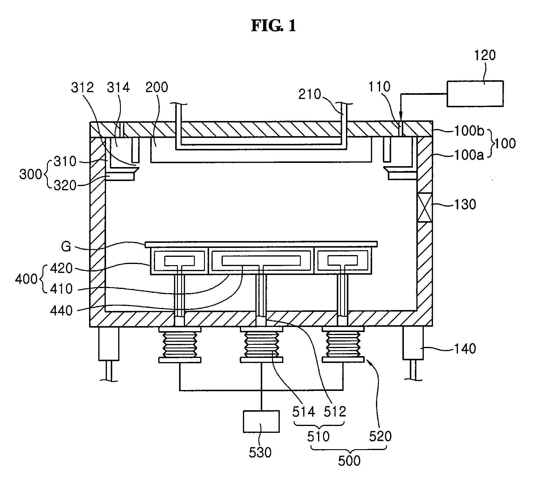
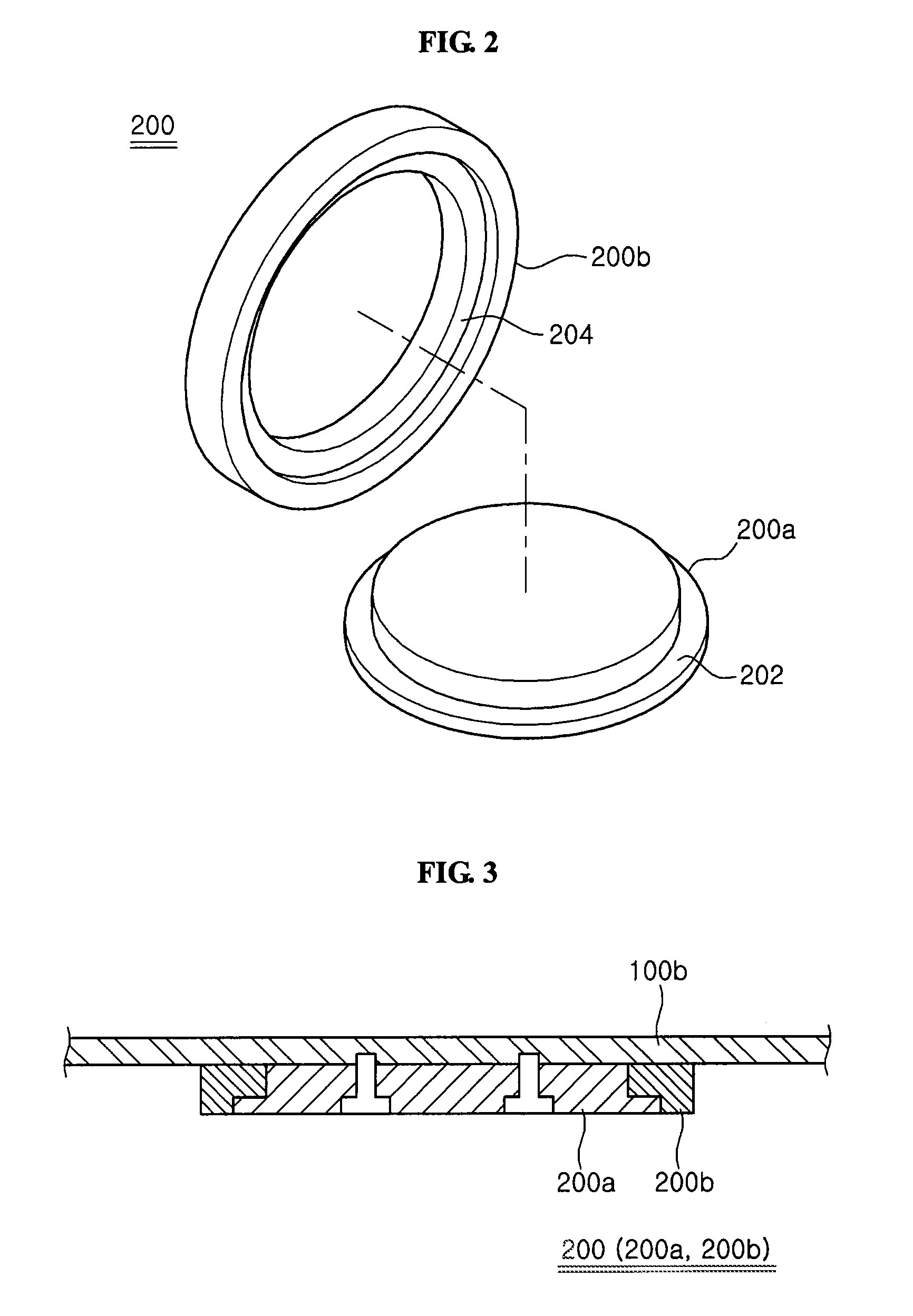
[0031]FIG. 1 is a cross-sectional view of a plasma processing apparatus according to a first exemplary embodiment of the present invention. FIG. 2 is a perspective view showing a variant of an insulating member provided in the plasma processing apparatus according to the first exemplary embodiment of the present invention. FIG. 3 is a cross-sectional view showing the insulating member of FIG. 2 attached to a chamber. FIG. 4 is a cross-sectional view of a first variant of the insulating member provided in the plasma processing apparatu...


PUM

PropertyMeasurementUnit
distanceaaaaaaaaaa
diameteraaaaaaaaaa
diameteraaaaaaaaaa

Abstract

A plasma processing apparatus includes: a chamber; an insulating member disposed in an upper portion of the chamber; a ground electrode formed at a side wall of the chamber, a ground potential being applied to the ground electrode; and a lower electrode disposed in a lower portion of the chamber, a substrate being placed on the lower electrode, wherein the lower electrode is divided into a plurality of electrodes.According to an aspect of the present invention, particles accumulated in the central portion on a lower surface, an edge area of an upper surface, a side, and an edge area of the lower surface of the substrate can be effectively removed.

Description

CROSS-REFERENCE TO RELATED APPLICATION[0001]This application is a continuation in part of pending U.S. patent application Ser. No. 11 / 947,610, filed Nov. 29, 2007, which claims priority to Korean Patent Application No. 10-2007-0109448, filed Oct. 30, 2007, Korean Patent Application No. 10-2007-0085561, filed Aug. 24, 2007, and to Korean Patent Application No. 10-2006-0124763, filed Dec. 8, 2006, the contents of which are incorporated herein by reference in their entirety.FIELD OF THE INVENTION[0002]The present invention relates to a plasma processing apparatus, particularly a plasma processing apparatus that removes a variety of impurities on a substrate.BACKGROUND OF THE INVENTION[0003]Semiconductor elements and flat panel displays are formed by depositing a plurality of thin films on a substrate and etching the films. That is, an element having a predetermined thin film pattern is formed by depositing thin films on a predetermined region of a substrate, mainly in the central regio...

Claims


Application Information

Patent Timeline
Patent Type & Authority Applications(United States)
IPC IPC(8): H01L21/306C23C16/44
CPCH01J37/32477H01J37/32724H01J37/32568H01J37/32522
Inventor KIM, SUNG RYUL
Owner TES CO LTD
Learn More