Magnetic device
a magnetic device and magnetic core technology, applied in the direction of transformer/inductance details, inductance with magnetic core, basic electric elements, etc., can solve the problems of reducing the thickness, reducing the inductance, and achieving sufficient characteristi
- Summary
- Abstract
- Description
- Claims
- Application Information
AI Technical Summary
Benefits of technology
Problems solved by technology
Method used
Image
Examples
embodiment 1
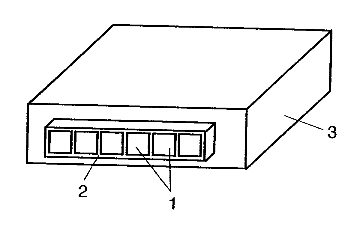
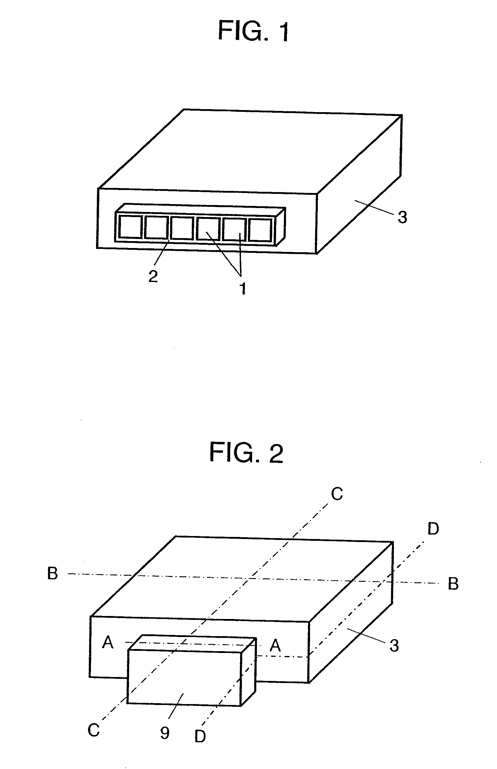
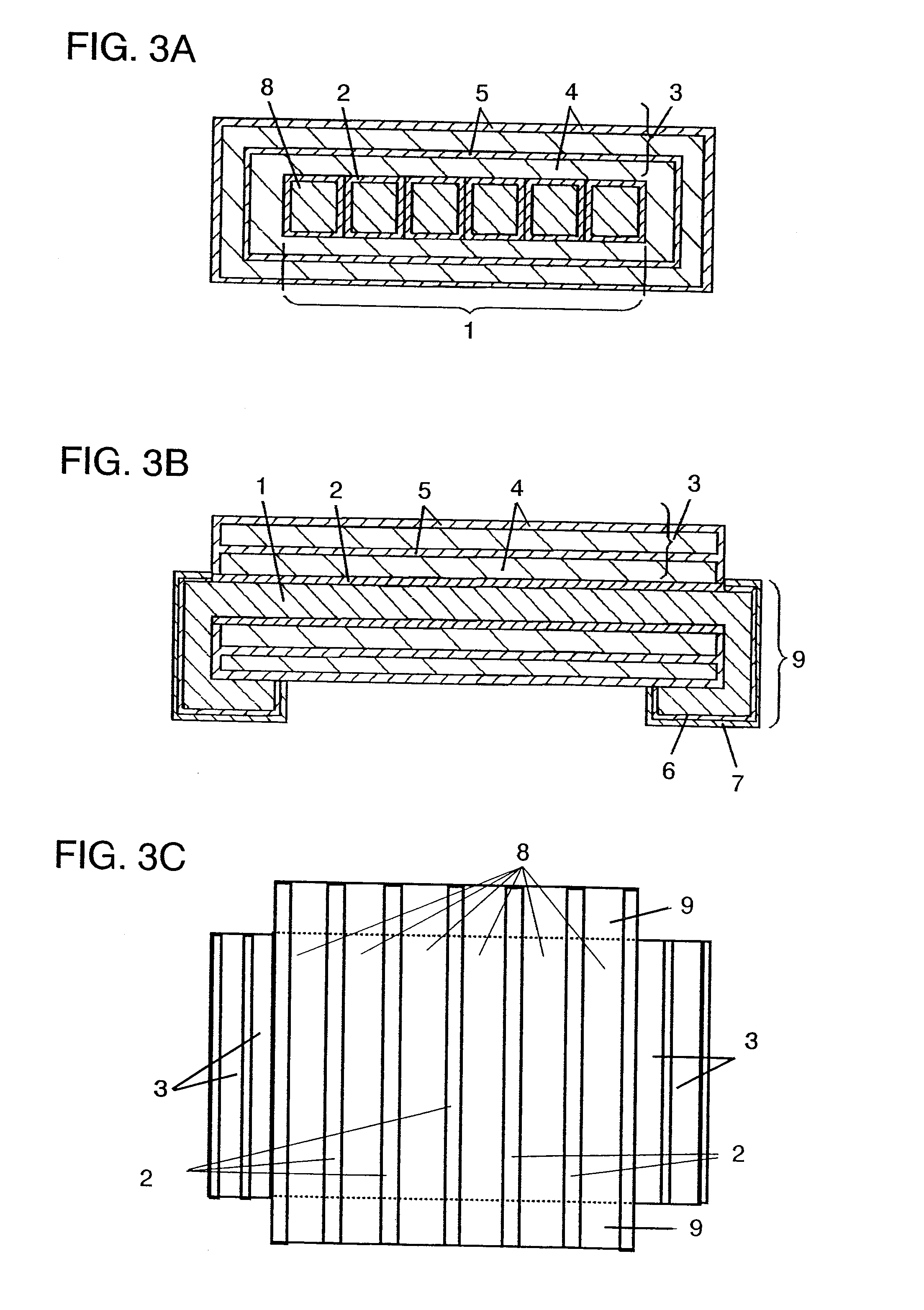
[0027]Embodiment 1 is to be described with reference to FIG. 1, FIG. 2 and FIG. 3A to FIG. 3C.
[0028]The coil conductor 1 comprises conductors 8 made of a metal material having low resistance covered with an insulation film 2 arranged in plurality.
[0029]In FIG. 3A to FIG. 3C, conductors 8 each covered with the insulation film 2 are arranged to be parallel to C-C direction in the same plane.
[0030]In the present embodiment six conductors 8 are employed, however, the number of conductors may be changed.
[0031]The reason of using such a constitution is as described below.
[0032]Generally, in a case where the coil conductor 1 is constituted with one conductor 8 by fabricating a metal material having low resistance such as a copper sheet or a copper wire, the current flowing through the conductor 8 flows concentrically at the surface of the conductor 8 as the frequency is higher by the skin effect. As a result, an apparent resistance value (Rac) of the coil conductor 1 increases at a high fr...
embodiment 2
[0058]Description is to be made to Embodiment 2 with reference to FIG. 2, FIG. 4 and FIG. 5.
[0059]The constitutions identical with those in Embodiment 1 carry the same reference numerals for which detailed descriptions will be omitted. Conductors 8 of a coil conductor 1 are covered each with insulation film 2. A coil conductor 1 shown in FIG. 4 is constituted with two stacked conductor layers. The conductor layer includes conductors 8 having rectangular cross sectional shapes are arranged in the same plane being parallel to the mounting surface.
[0060]A coil conductor 1 shown in FIG. 5 is different from FIG. 4 in that conductors 8 are arranged in the parallel direction to line D-D shown in FIG. 2.
[0061]The material for the conductor 8 is preferably copper, silver or aluminum of low specific resistivity, or it may be an alloy containing them. Further, the insulation film layer 2 electrically insulates each of the conductors 8.
[0062]Since a connection terminal 9 is formed contiguous wi...
embodiment 3
[0080]Embodiment 3 is to be described with reference to FIG. 2 and FIG. 6.
[0081]As shown in FIG. 2 and FIG. 6, a coil conductor 1 of a magnetic device comprises two rectangular conductors 8 formed by dividing in the vertical direction relative to the mounting surface. Further, since the basic constitution of this embodiment is identical with those of Embodiments 1 and 2, detailed descriptions therefor will be omitted.
[0082]However, this is different from Embodiments 1 and 2 in that a slit 11 is formed in the magnetic layer 4 cutting the magnetic layer 4. The slit 11 can be filled with an insulating material. The slit 11 can suppress the saturation of the magnetic flux and improve the DC superimpose characteristic.
[0083]The operation of the magnetic device having the foregoing constitution is to be described below.
[0084]When a high current is supplied to the coil conductor 1, a strong magnetic flux is generated in the magnetic device to generate a magnetic flux in the direction of th...
PUM
| Property | Measurement | Unit |
|---|---|---|
| width | aaaaa | aaaaa |
| current | aaaaa | aaaaa |
| frequency | aaaaa | aaaaa |
Abstract
Description
Claims
Application Information
 - R&D
- Intellectual Property
- Life Sciences
- Materials
- Tech Scout
- Unparalleled Data Quality
- Higher Quality Content
- 60% Fewer Hallucinations
Browse by: Latest US Patents, China's latest patents, Technical Efficacy Thesaurus, Application Domain, Technology Topic, Popular Technical Reports.
© 2025 PatSnap. All rights reserved.Legal|Privacy policy|Modern Slavery Act Transparency Statement|Sitemap|About US| Contact US: help@patsnap.com


