Package structure
a technology of led package structure and packaging, applied in the direction of basic electric elements, electrical apparatus, semiconductor devices, etc., can solve the problems of deteriorating the luminescence efficiency of led package structure and often damaged leds, and achieve the effect of superior luminance efficiency
- Summary
- Abstract
- Description
- Claims
- Application Information
AI Technical Summary
Benefits of technology
Problems solved by technology
Method used
Image
Examples
Embodiment Construction
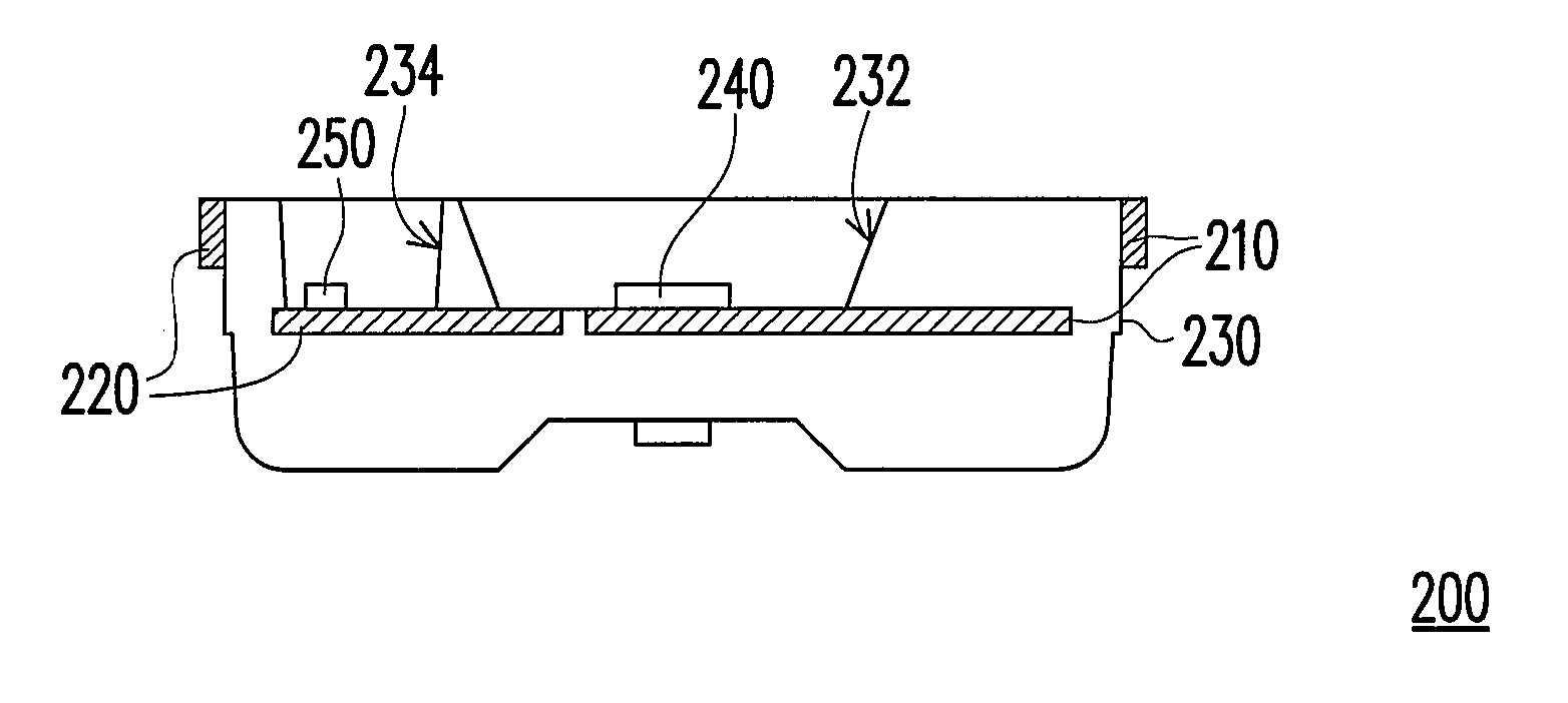
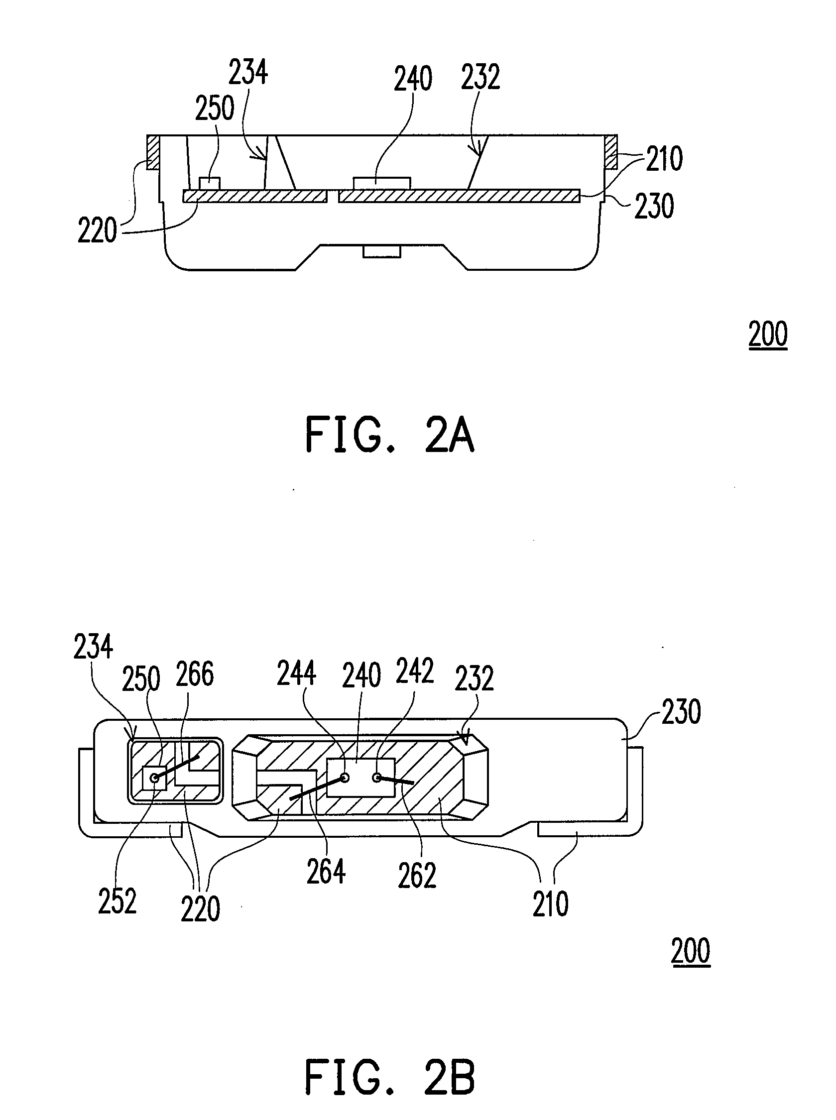
[0030]FIG. 2A is a cross-sectional schematic view depicting a package structure according to one embodiment of the present invention, while FIG. 2B is a top view depicting the package structure of FIG. 2A. Referring to FIGS. 2A and 2B, the package structure 200 of the present embodiment includes a first lead 210, a second lead 220, an encapsulant 230, a light-emitting device 240, and an electrostatic discharge (ESD) protection device 250. The second lead 220 is disposed beside the first lead 210, and parts of the first lead 210 and the second lead 220 are packaged by the encapsulant 230. The encapsulant 230 has a first cavity 232 and a second cavity 234. Here, parts of the first lead 210 and the second lead 220 are exposed by the first cavity 232, and the other parts of the first lead 210 and the second lead 220 are exposed by the second cavity 234. In addition, the light-emitting device 240 is disposed inside the first cavity 232 and electrically connected to the first lead 210 and...
PUM
 Abstract
Description
Claims
Application Information
 - R&D
- Intellectual Property
- Life Sciences
- Materials
- Tech Scout
- Unparalleled Data Quality
- Higher Quality Content
- 60% Fewer Hallucinations
Browse by: Latest US Patents, China's latest patents, Technical Efficacy Thesaurus, Application Domain, Technology Topic, Popular Technical Reports.
© 2025 PatSnap. All rights reserved.Legal|Privacy policy|Modern Slavery Act Transparency Statement|Sitemap|About US| Contact US: help@patsnap.com


