
Method of Layout of a Driving Chip of a Liquid Crystal Display and Related Liquid Crystal Display

a technology of liquid crystal display and driving chip, which is applied in the direction of non-linear optics, static indicating devices, instruments, etc., can solve the problems that the layout shown in fig. 3 is not great help in reducing the area of the substrate, and the margin area of the bottom of the lcd b>10/b> cannot be reduced effectively, so as to reduce the size of the lcd

Active Publication Date: 2008-05-01
NOVATEK MICROELECTRONICS CORP
View PDF1 Cites 13 Cited by
  • Summary
  • Abstract
  • Description
  • Claims
  • Application Information

AI Technical Summary

Benefits of technology

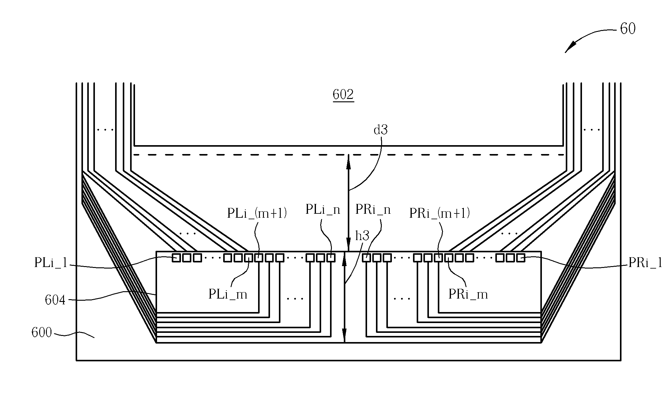
[0009]According to the claimed invention, a method of layout of a driving chip of an LCD, for reducing a size of the LCD, comprises forming a first pin group comprising a plurality of pins for outputting gate driving signals along a first direction; forming a second pin group comprising a plurality of pins for outputting gate driving signals along the first dire...

Problems solved by technology

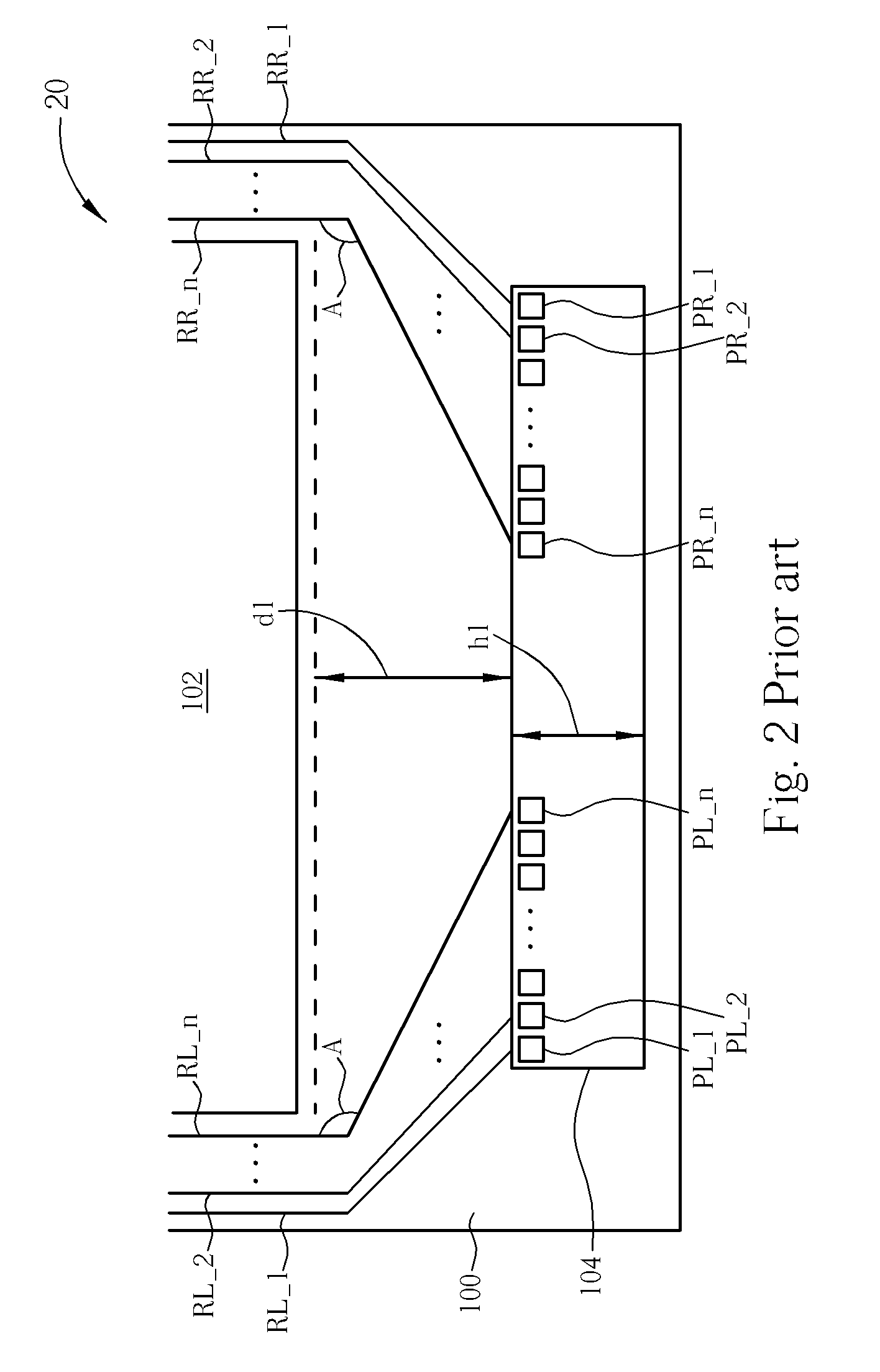
Thus, the layout shown in FIG. 3 is no great help for reducing the area of the substrate 100.
Therefore, no matter applying the layout of FIG. 2 or FIG. 3, the margin area of the bottom of the LCD 10 cannot be reduced effectively.

Method used


Image

  • Method of Layout of a Driving Chip of a Liquid Crystal Display and Related Liquid Crystal Display
  • Method of Layout of a Driving Chip of a Liquid Crystal Display and Related Liquid Crystal Display
  • Method of Layout of a Driving Chip of a Liquid Crystal Display and Related Liquid Crystal Display

Examples


Embodiment Construction

[0018]Please refer to FIG. 4. FIG. 4 is a schematic diagram of a layout process 40 of a driving chip of an LCD in accordance with an embodiment of the present invention. The layout process 40 can reduce the size of the LCD, and comprises the following steps:

[0019]Step 400: start.

[0020]Step 402: form a first pin group comprising a plurality of pins for outputting gate driving signals along a first direction.

[0021]Step 404: form a second pin group comprising a plurality of pins for outputting gate driving signals along the first direction.

[0022]Step 406: form a first wire group comprising a plurality of wires each coupled between a pin of the first pin group and a panel of the LCD.

[0023]Step 408: form a second wire group comprising a plurality of wires each coupled between a pin of the second pin group and the panel, wherein each wire of the second wire group comprises at least a bend formed inside the driving chip.

[0024]Step 410: end.

[0025]In the process 40, the first wire group is c...


PUM


Abstract

A method of layout of a driving chip of an LCD, for reducing a size of the LCD, includes forming a first pin group including a plurality of pins utilized for outputting gate driving signals along a first direction, forming a second pin group including a plurality of pins utilized for outputting gate driving signals along the first direction, forming a first wire group including a plurality of wires each coupled between a pin of the first pin group and a panel of the LCD, and forming a second wire group including a plurality of wires each coupled between a pin of the second pin group and the panel, wherein each wire of the second wire group includes at least a bender formed inside the driving chip.

Description

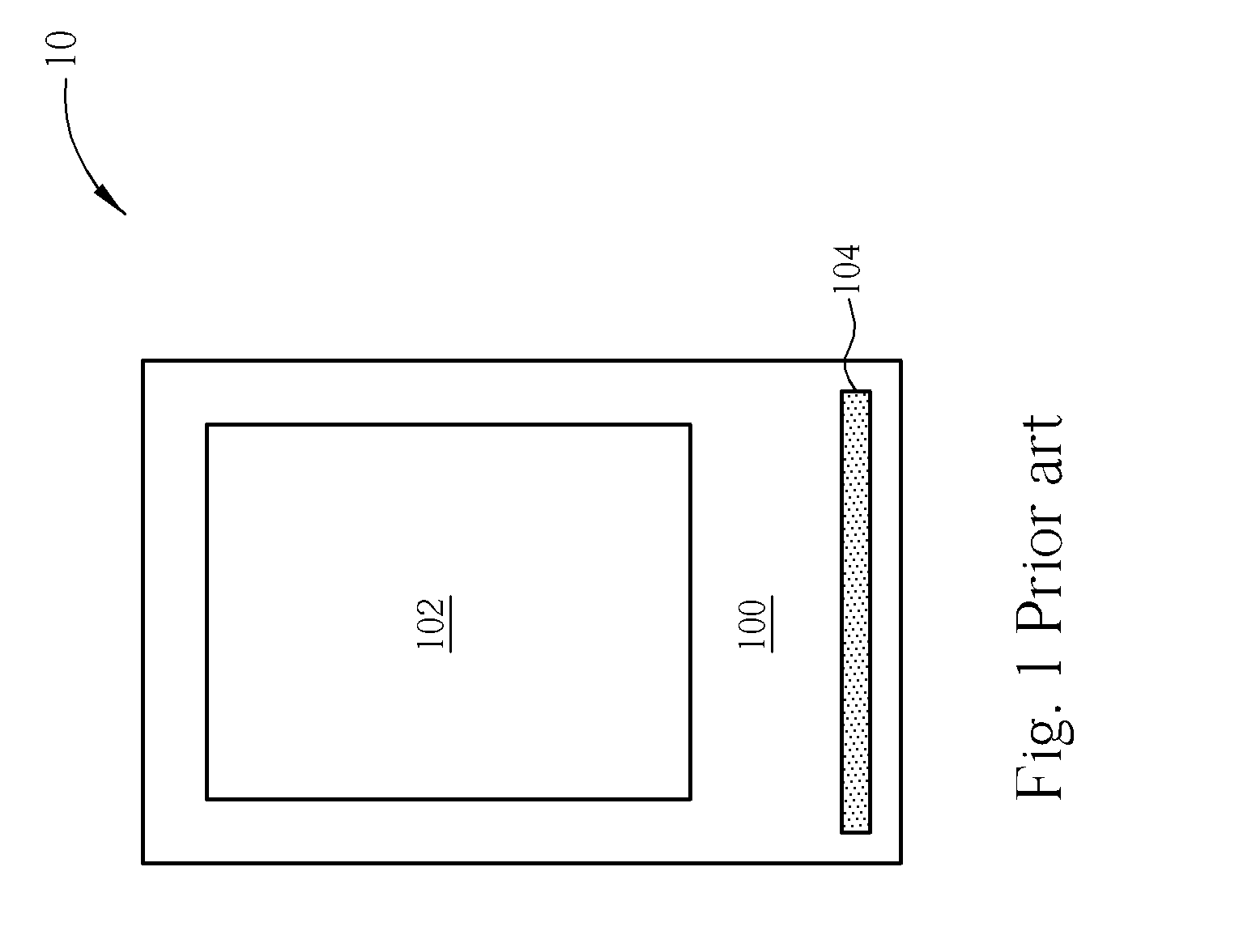
BACKGROUND OF THE INVENTION[0001]1. Field of the Invention[0002]The present invention relates to a method of layout of a driving chip of an liquid crystal display (LCD) and related LCD, and more particularly, to a layout method and related LCD capable of reducing the margin-area width of the bottom of the substrate of the LCD.[0003]2. Description of the Prior Art[0004]The advantages of a liquid crystal display (LCD) include light weight, less power consumption, and less radiation contamination. Thus, the LCD monitors have been widely applied to various portable electronic products, such as notebooks, PDAs, etc. Generally, the portable electronic products have to be designed as small as possible. Therefore, the prior art has already provided many layout methods for reducing layout sizes of the LCDs in the portable electronic products.[0005]Please refer to FIG. 1. FIG. 1 is a schematic diagram of a prior art LCD 10 of a portable electronic device. The LCD 10 includes a substrate 100, ...

Claims


Application Information

Patent Timeline
IPC IPC(8): G09G3/36
CPCG02F1/1345G02F1/13452G09G2310/0278G09G2300/0426G09G3/3611
Inventor TSENG, CHING-WU
Owner NOVATEK MICROELECTRONICS CORP
Learn More