
Substrate processing method and storage medium having program stored therein

a processing method and program technology, applied in the direction of adaptive control, instruments, nuclear elements, etc., can solve the problems of reducing throughput, wafer transfer processing will have been executed in vain, etching process cannot be executed in the processing chamber, etc., to achieve the desired level of throughput and improve the adjustment accuracy

Active Publication Date: 2008-04-17
TOKYO ELECTRON LTD
View PDF9 Cites 4 Cited by
  • Summary
  • Abstract
  • Description
  • Claims
  • Application Information

AI Technical Summary

Benefits of technology

[0010] An object of the present invention having been completed by addressing the issues of the related art discussed above is to provide a substrate processing method and a storage medium having a program stored therein with which processing target substrates can be transferred and processed continuously while maintaining a desired level of throughput by eliminating superfluous transfer of processing target substrates and an improvement in the accuracy of processing parameter adjustment achieved through feedforward calculation, is assured.
[0013] According to the present invention described above, in which a decision is made as to whether or not the processing parameter value calculated in the first processing parameter calculation (first calculation) is within the allowable range, the processing target substrate is transferred to the processing chamber only if it is decided that the processing target substrate should be transferred to the processing chamber. As a result, the problematic situation which tends to occur in the related art, whereby a processing target substrate having been already transferred to the processing chamber cannot be processed with the processing parameter value judged to be beyond the allowable range, can be prevented. In other words, a superfluous execution of processing target substrate transfer processing is prevented. In addition, in the second processing parameter calculation (second calculation), a processing parameter value can be determined by reflecting the adjustment value determined based upon the most recent processing executed in the processing chamber, achieving an improvement in the processing parameter adjustment accuracy. Furthermore, the processing parameter value calculated in the first feedforward calculation (first calculation) is not intended to be used in the actual execution of processing target substrate processing and thus, the preprocessing surface profile measurement can be executed while the immediately preceding processing target substrate is being processed, allowing the substrate transfer processing to be executed without lowering the throughput.
[0014] Moreover, upon completing the processing in the processing chamber, a postprocessing measurement phase, in which the processing target substrate having been processed is carried into the measurement chamber and the postprocessing surface profile is measured and an adjustment value calculation phase, in which the adjustment value to be used to adjust the processing parameter value is calculated based upon the postprocessing surface profile measurement value are executed. Thus, a processing parameter value reflecting the latest adjustment value can be determined when processing the next processing target substrate, which assures an improvement in the processing parameter adjustment accuracy.
[0018] According to the present invention in which values of the processing parameter are calculated for the individual processing chambers through the first processing parameter calculation (first calculation) and a decision is made as to whether or not each processing parameter value calculated in correspondence to one of the processing chambers, is within the allowable range, the processing target substrate is transferred only to a processing chamber with a processing parameter value judged to be within the allowable range by making a decision prior to the actual processing target substrate transfer to the processing chamber as to whether or not the transfer processing should be executed. As a result, superfluous execution of processing target substrate transfer processing is prevented. In addition, in the second processing parameter calculation (second calculation), a processing parameter value reflecting the adjustment value determined based upon the most recent processing having been executed in the specific processing chamber where the processing target substrate is to be processed shortly can be calculated, assuring an improvement in the processing parameter adjustment accuracy.
[0020] According to the present invention described above, after a processing parameter value is recalculated in the second calculation phase, a decision is made in the second decision-making phase as to whether or not the recalculated processing parameter value is within the allowable range and if the value is judged to be outside the allowable range, the processing target substrate is transferred to another processing chamber, the processing parameter value of which has been judged in the first decision-making phase to be within the allowable range. As a result, superfluous execution of the transfer processing is prevented.
[0022] The present invention provides a substrate processing apparatus and a storage medium with a program stored therein, with which processing target substrates can be transferred and processed continuously while maintaining a desired level of throughput by eliminating superfluous transfer of processing target substrates and an improvement in the adjustment accuracy is assured for the processing parameter calculated through feedforward calculation.

Problems solved by technology

While it may appear that the feedforward calculation should be executed by transferring the subsequent wafer, i.e., the second wafer, to the measurement chamber after completing the feedback calculation executed based upon the processing results for the first wafer most recently processed in the processing chamber, this is bound to result in a greatly reduced throughput since the next wafer is carried into the measurement chamber for the preprocessing measurement only after the post-processing measurement for the preceding wafer is completed.
However, this alternative is problematic in that if the value of the processing parameter (e.g., the etching time) is determined to be beyond the allowable range at the time of the feedforward calculation, the etching process cannot be executed in the processing chamber and thus, the wafer transfer processing will have been executed in vain.

Method used


Image

  • Substrate processing method and storage medium having program stored therein
  • Substrate processing method and storage medium having program stored therein
  • Substrate processing method and storage medium having program stored therein

Examples


Embodiment Construction

[0037] The following is a detailed explanation of a preferred embodiment of the present invention, given in reference to the attached drawings. It is to be noted that in the description and the drawings, the same reference numerals are assigned to components having substantially identical functions and structural features to preclude the necessity for a repeated explanation thereof.

(Structural Example for Substrate Processing Apparatus)

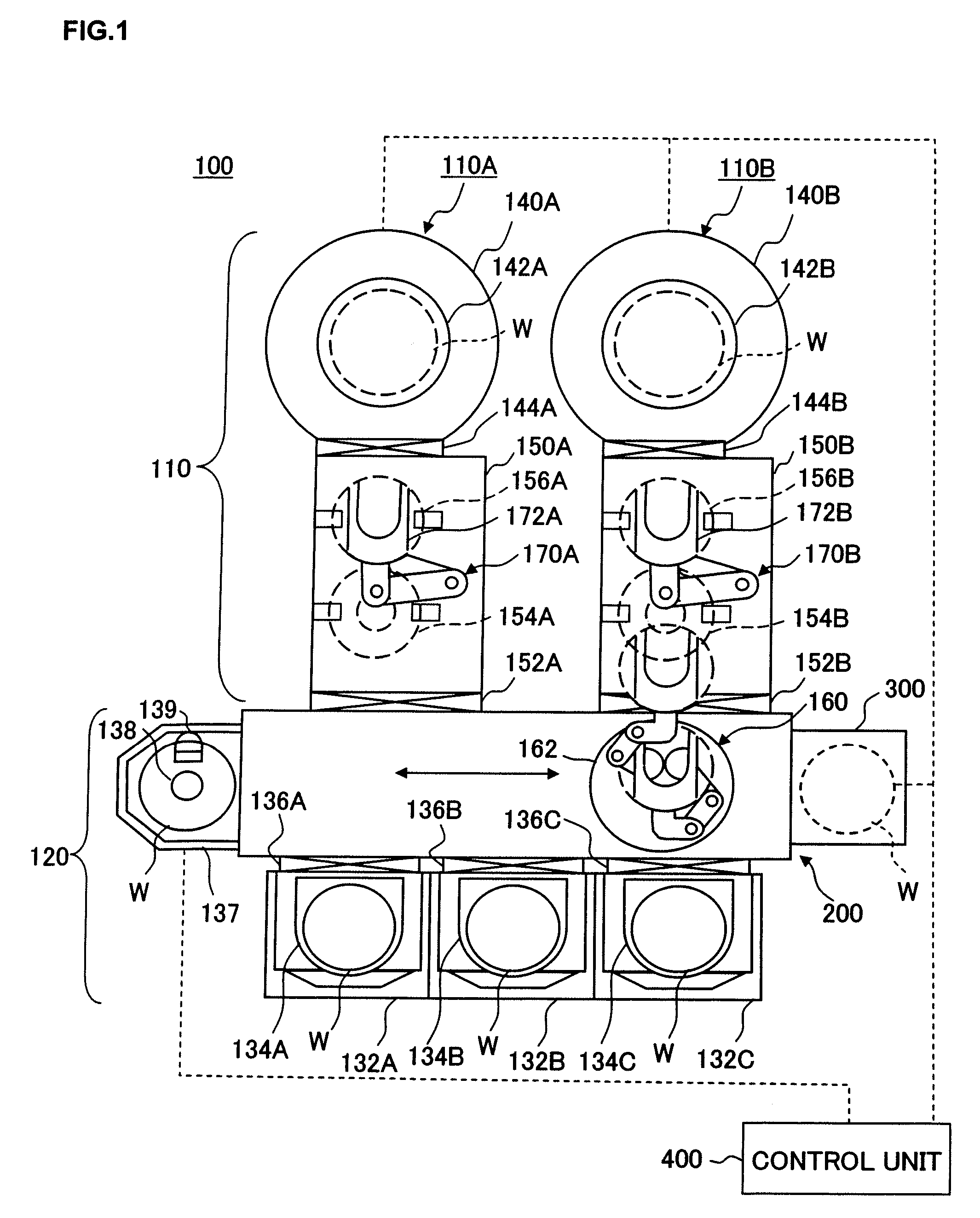
[0038] First, a structural example that may be adopted in the substrate processing apparatus in the embodiment of the present invention is explained in reference to a drawing. The substrate processing apparatus in this example includes at least one vacuum processing unit connected to a transfer chamber. FIG. 1 is a sectional view schematically illustrating the structure of the substrate processing apparatus achieved in the embodiment.

[0039] The substrate processing apparatus 100 includes either a single vacuum processing unit 110 or a plurality of...


PUM


Abstract

First feedforward calculation is executed when a preprocessing surface profile is measured and a processing chamber with its processing parameter value having been obtained through the first feedforward calculation judged to be within an allowable range is determined. Wafer transfer is executed only in conjunction with a processing chamber having a processing parameter value judged to be within the allowable range, and the wafer is carried to the entry point of the processing chamber. Then, second feedforward calculation is executed by reflecting the results of feedback calculation executed based upon the most recent processing having been executed in the particular processing chamber and wafer processing is executed in the processing chamber based upon the processing parameter value calculated in the second feedforward calculation.

Description

CROSS-REFERENCE TO RELATED APPLICATIONS [0001] This document claims priority to Japanese Patent Application Number 2006-273793, filed on Oct. 5, 2006 and U.S. Provisional Application No. 60 / 870,789, filed on Dec. 19, 2006, the entire content of which are hereby incorporated by reference.FIELD OF THE INVENTION [0002] The present invention relates to a substrate processing method to be adopted when executing a specific type of processing such as etching on a surface of a processing target substrate such as a semiconductor wafer and a storage medium having a program stored therein. BACKGROUND OF THE INVENTION [0003] Ever finer design details need to be satisfied in today's semiconductor integrated circuit design rules by assuring a higher level of dimensional accuracy in circuit patterns formed at the surfaces of semiconductor wafers (hereafter may be simply referred to as “wafers”). When a plurality of wafers is processed continuously, conditions inside the processing chamber graduall...

Claims


Application Information

Patent Timeline
Patent Type & Authority Applications(United States)
IPC IPC(8): G05B13/02
CPCH01L21/67745H01L21/67276
Inventor KUBOTA, SHIGERUSAKANO, SHINJI
Owner TOKYO ELECTRON LTD
Learn More