Level-shifting circuits and methods of level shifting

Inactive Publication Date: 2008-02-14
SAMSUNG ELECTRONICS CO LTD
View PDF5 Cites 10 Cited by
  • Summary
  • Abstract
  • Description
  • Claims
  • Application Information

AI Technical Summary

Benefits of technology

[0030]The present invention increases a

Problems solved by technology

Therefore, when using a conventional level shifter, operating margins of the semiconductor ICs may decrease and operating capabilities of the semiconductor ICs may be degraded.
Accordingly, decreasing the power voltage of the internal circuits causes a problem in that the operating margin of the latch is also decreased.

Method used


Image

  • Level-shifting circuits and methods of level shifting
  • Level-shifting circuits and methods of level shifting
  • Level-shifting circuits and methods of level shifting

Examples


Embodiment Construction

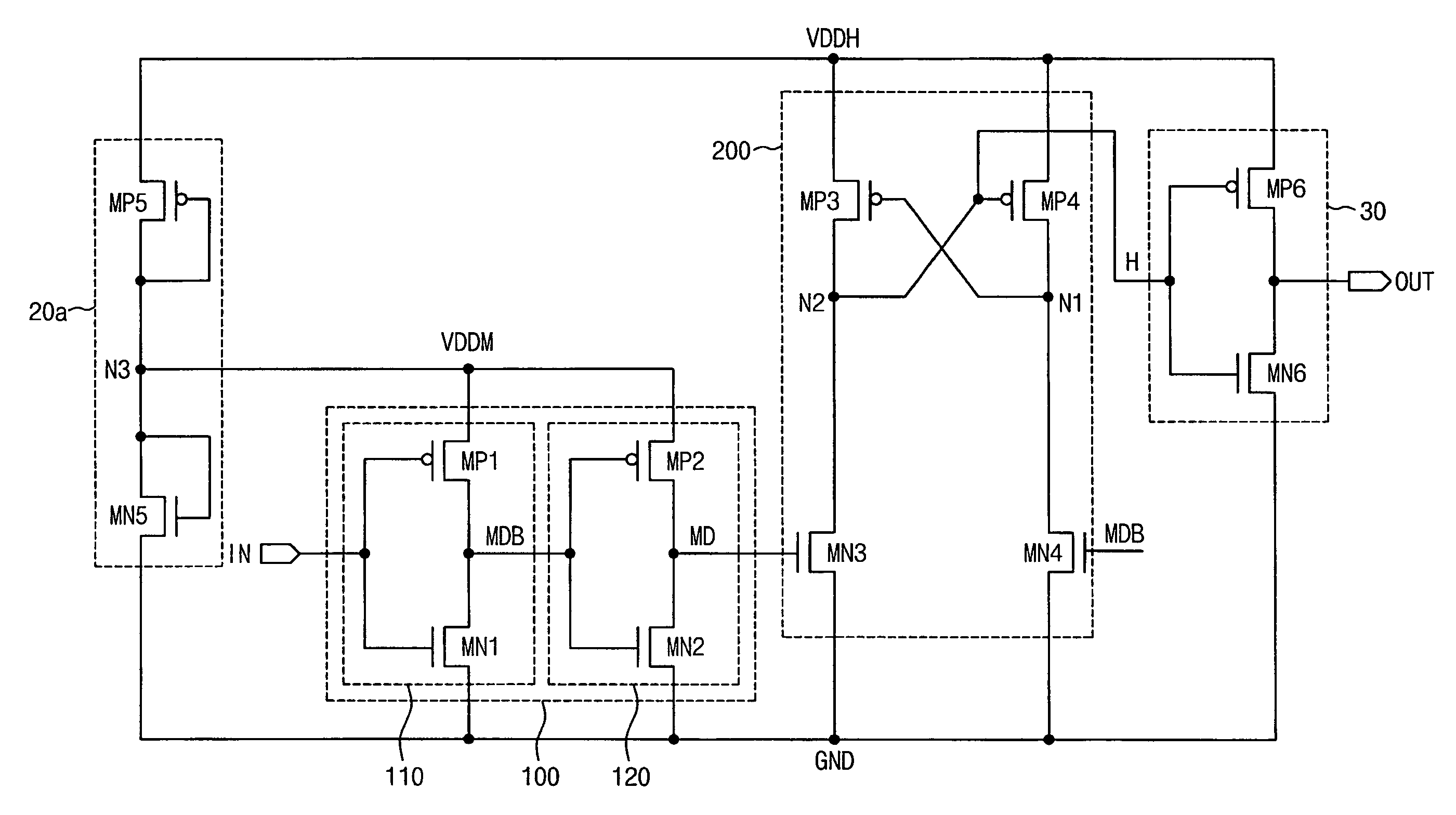
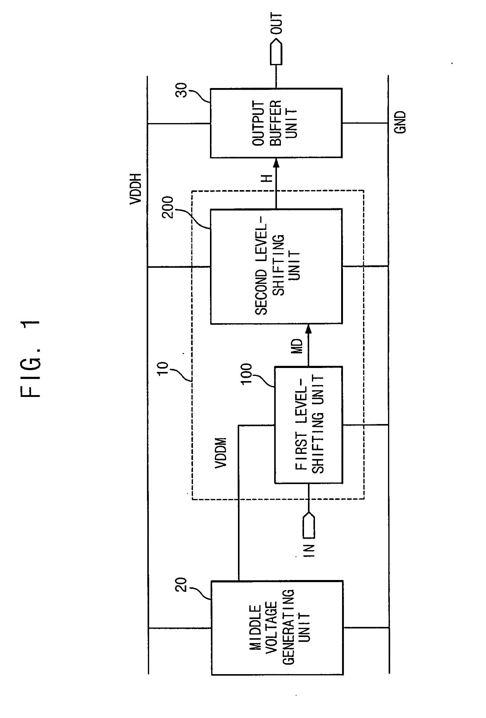
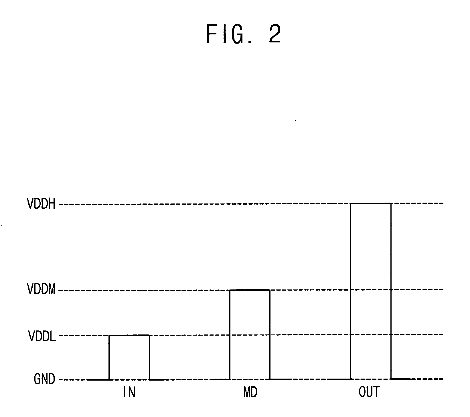
[0037]Embodiments of the present invention now will be described more fully with reference to the accompanying drawings, in which embodiments of the invention are shown. This invention may, however, be embodied in many different forms and should not be construed as limited to the embodiments set forth herein. Rather, these embodiments are provided so that this disclosure will be thorough and complete.

[0038]It will be understood that, although the terms first, second, etc. may be used herein to describe various elements, these elements should not be limited by these terms. These terms are used to distinguish one element from another. For example, a first element could be termed a second element, and, similarly, a second element could be termed a first element, without departing from the scope of the present invention. As used herein, the term “and / or” includes any and all combinations of one or more of the associated listed items.

[0039]It will be understood that when an element is re...


PUM


Abstract

A level-shifting circuit includes a level shifter and a middle voltage generating unit. The level shifter generates a middle voltage signal by level-shifting a first signal. The middle voltage signal swings between a level of a ground voltage and a level of a middle voltage, and the first signal swings between the level of the ground voltage and a level of a first voltage. In addition, the level shifter generates a second signal by level-shifting the middle voltage signal. The second signal swings between the level of the ground voltage and a level of a second voltage. The middle voltage generating unit generates the middle voltage by receiving the second voltage and the ground voltage. Therefore, the level-shifting circuit increases an operating margin of an input voltage.

Description

CROSS-REFERENCE TO RELATED APPLICATIONS[0001]This application claims priority under 35 USC §119 to Korean Patent Application No. 10-2006-0075953, filed on Aug. 11, 2006 in the Korean Intellectual Property Office (KIPO), the contents of which are incorporated herein by reference in their entirety.BACKGROUND OF THE INVENTION[0002]1. Field of the Invention[0003]The present invention relates to semiconductor devices, and more particularly to level-shifting circuits and methods of level shifting.[0004]2. Description of the Related Art[0005]Most semiconductor integrated circuits (ICs) include internal circuits for performing internal functions and interface circuits for interfacing with external circuits. Also, the semiconductor ICs include a power supply device for providing a power voltage to the internal circuits and the interface circuits. Most of the internal circuits use a power voltage below 1.0 V, but most of the interface circuits use a power voltage over 1.0V(e.g., 1.8V or 2.5V)...

Claims


Application Information

Patent Timeline
IPC IPC(8): H03L5/00
CPCH03K3/35613G11C5/14
Inventor CHUNG, DAE-YOUNGKIM, SANG-KYU
Owner SAMSUNG ELECTRONICS CO LTD
Why Eureka
Try Eureka