Motion Detection Imaging Device
- Summary
- Abstract
- Description
- Claims
- Application Information
AI Technical Summary
Benefits of technology
Problems solved by technology
Method used
Image
Examples
first embodiment
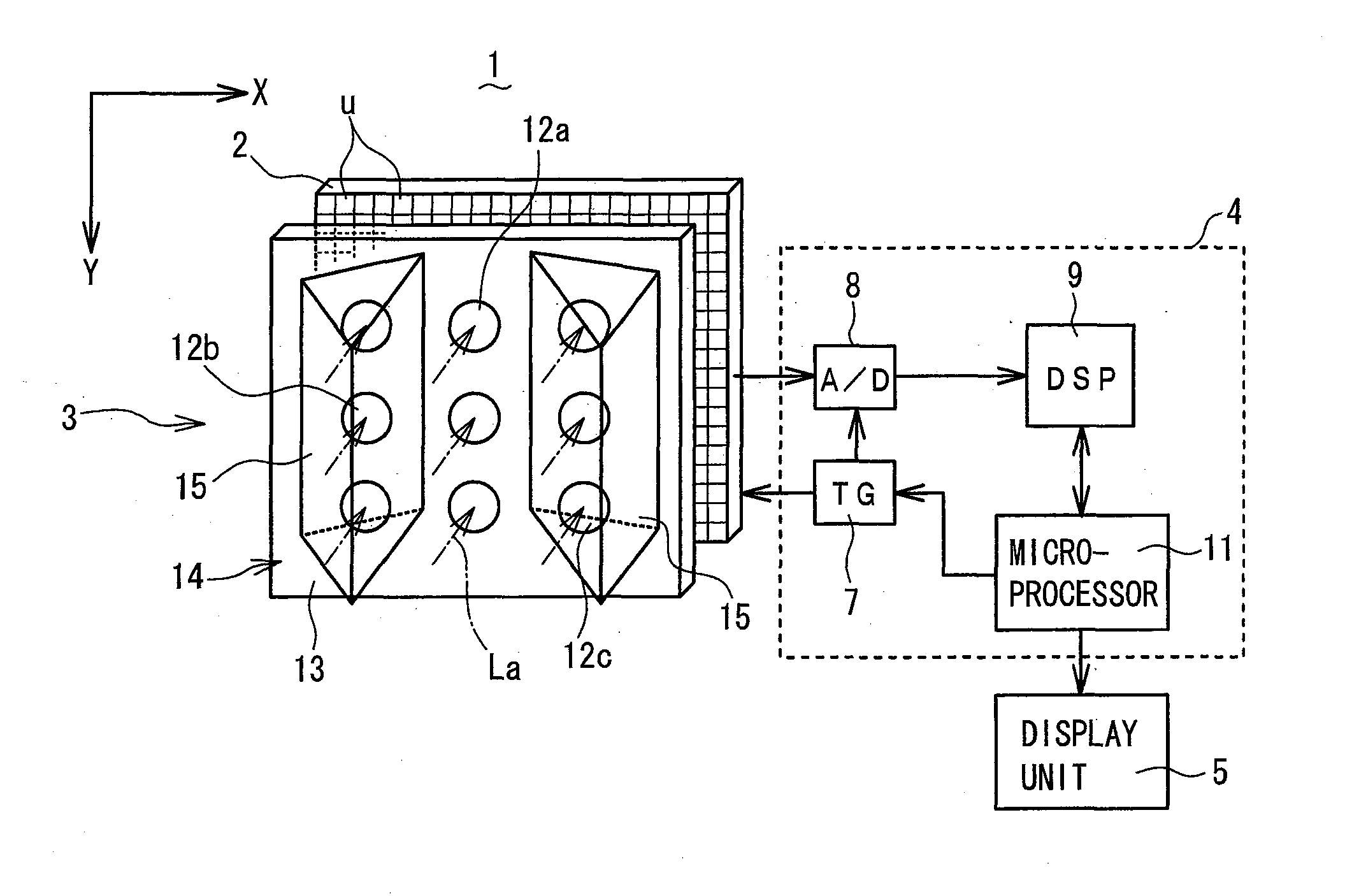
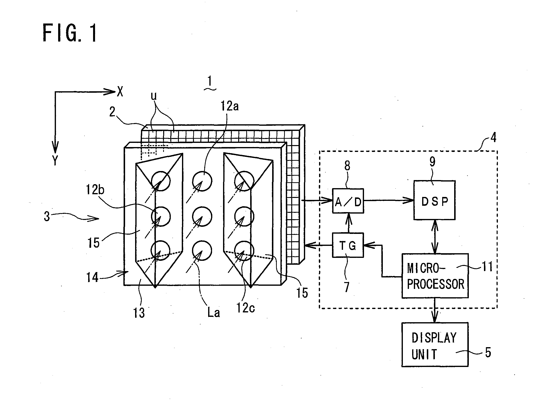
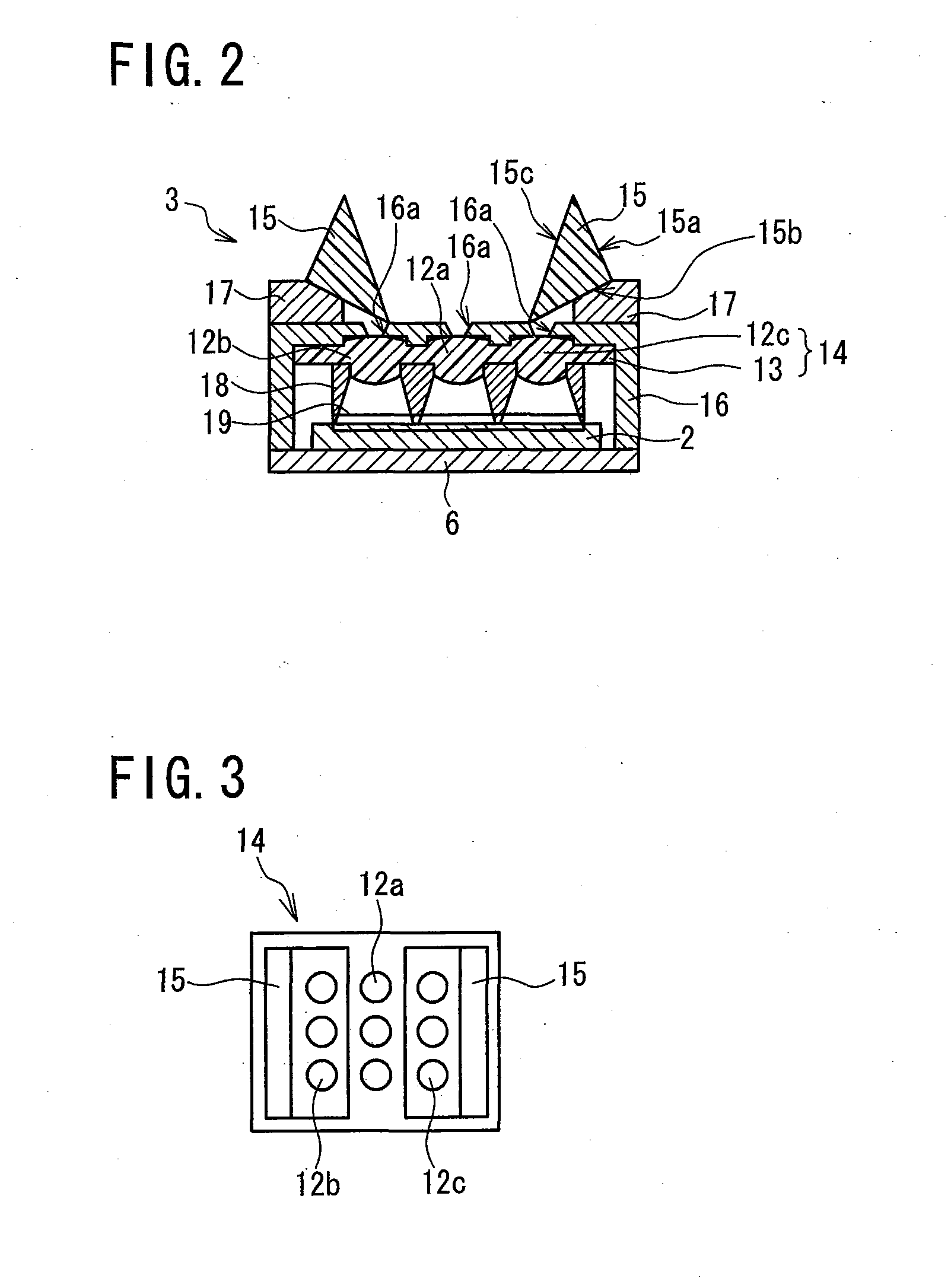
[0032]Referring to FIG. 1 to FIG. 8, a motion detection imaging device (imaging device for motion detection) 1 according to a first embodiment of the present invention will be described. FIG. 1 is a schematic perspective view of the motion detection imaging device 1 including a solid-state imaging element 2 and an optical lens system 3, while FIG. 2 is a schematic bottom cross-sectional view of the motion detection imaging device 1 of FIG. 1. As shown in FIG. 1, the motion detection imaging device 1 comprises: a solid-state imaging element (photodetector array) 2 having unit pixels “u” arranged in a matrix of rows and columns (X and Y directions); and an optical lens system 3 for collecting light entering in a front capture range (picture-taking range) of 120° so as to form images on the solid-state imaging element 2. The motion detection imaging device 1 further comprises: a motion detection circuit 4 for reading the formed images on the solid-state imaging element 2 as image infor...
second embodiment
[0057]Referring to FIG. 9, a motion detection device 1 according to a second embodiment of the present invention will be described. The motion detection device 1 of the second embodiment is similar to that of the first embodiment, except that 30-60-90 degree right-angle prisms 215 (claimed “light bending means”) are placed on the entrance side of the optical lens array 14 here in place of the 45-45-90 degree right-angle prisms 15 used in the first embodiment. FIG. 9 is a schematic optical path diagram of an optical lens system 203 of the motion detection device 1 according to the second embodiment as seen from the bottom thereof, showing a light flux passing through each of the optical lenses 12a, 12b, 12c. Similarly as in the first embodiment, the optical lens system 203 has an optical lens array 14 of optical lenses 12a, 12b, 12c and a solid-state imaging element 2. Thus, description of parts similar to those in the first embodiment is omitted where appropriate.
[0058]As shown in F...
third embodiment
[0062]Referring next to FIG. 10, a motion detection device 1 according to a third embodiment of the present invention will be described. The motion detection device 1 of the third embodiment is similar to that of the first embodiment, except that the nine optical lenses 12a, 12b, 12c have a capture range of 60° or approximately 60° (which importantly is not larger than approximately 60°) to expand the capture range of the optical lens system 3 of the first embodiment to approximately 180°, and that equilateral triangle prisms 315 (claimed “light bending means”) for guiding light are placed on the light entrance side of an optical lens array 14 in place of the 45-45-90 degree right-angle prisms 15 of the first embodiment. FIG. 10 is a schematic optical path diagram of an optical lens system 303 of the motion detection imaging device 1 according to the third embodiment as seen from the bottom thereof, showing a light flux passing through each of the optical lenses 12a, 12b, 12c. Simil...
PUM
 Abstract
Description
Claims
Application Information
 - R&D
- Intellectual Property
- Life Sciences
- Materials
- Tech Scout
- Unparalleled Data Quality
- Higher Quality Content
- 60% Fewer Hallucinations
Browse by: Latest US Patents, China's latest patents, Technical Efficacy Thesaurus, Application Domain, Technology Topic, Popular Technical Reports.
© 2025 PatSnap. All rights reserved.Legal|Privacy policy|Modern Slavery Act Transparency Statement|Sitemap|About US| Contact US: help@patsnap.com


