
Panel assembly

a panel and assembly technology, applied in the field of panel assembly, can solve the problems of deteriorating resolution of display panels, affecting the overall manufacturing process, and reducing the productivity of the produ

Inactive Publication Date: 2007-11-22
SAMSUNG DISPLAY CO LTD
View PDF6 Cites 109 Cited by
  • Summary
  • Abstract
  • Description
  • Claims
  • Application Information

AI Technical Summary

Benefits of technology

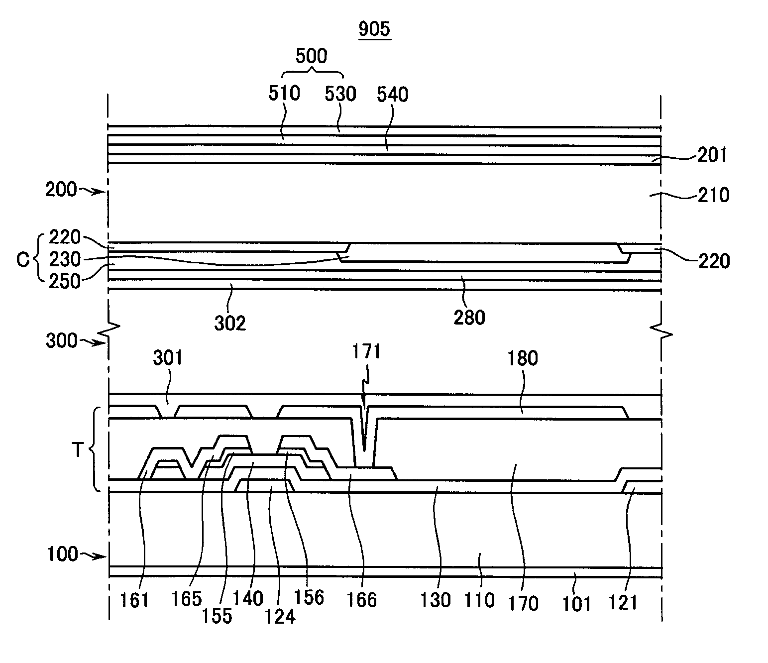
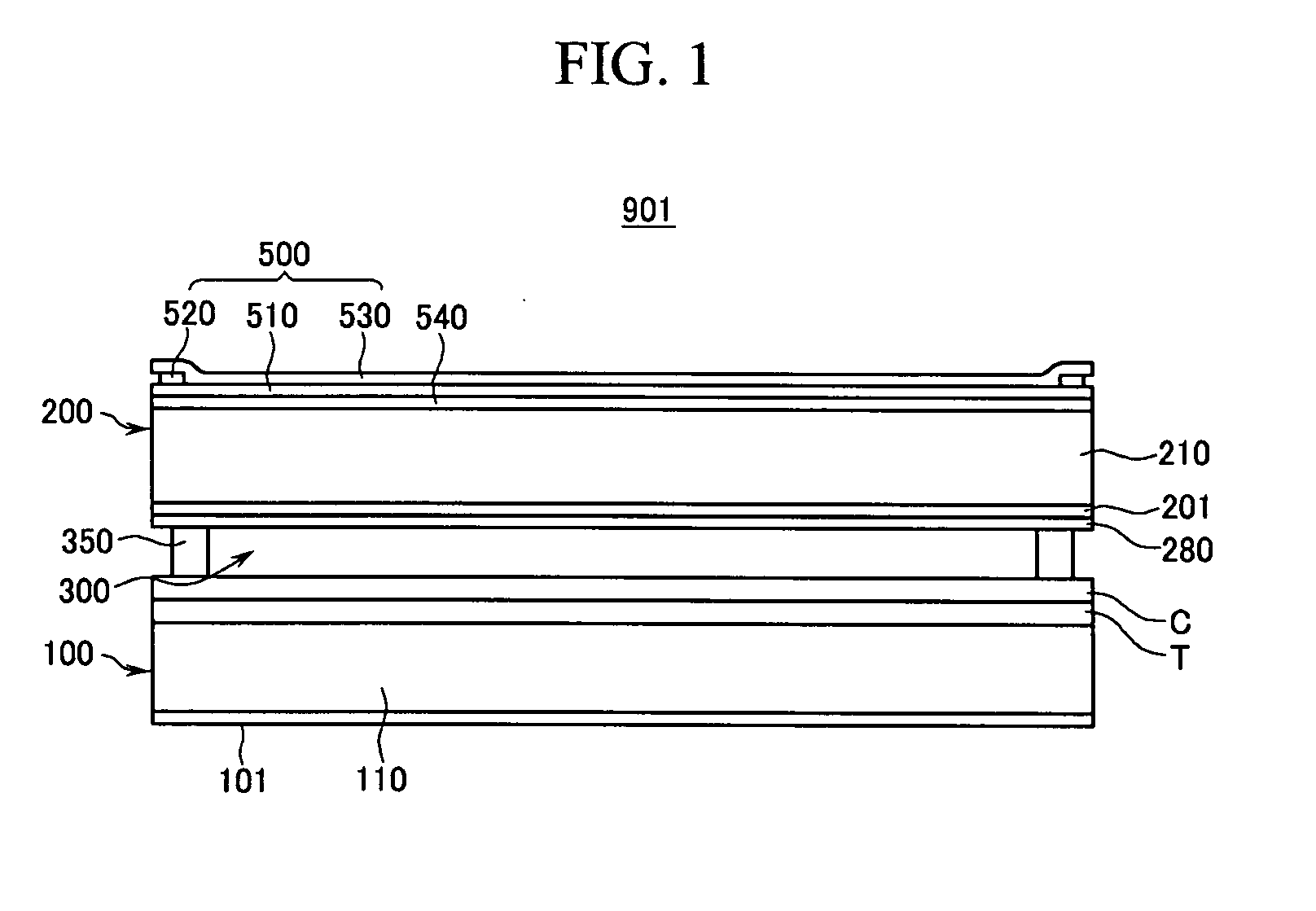
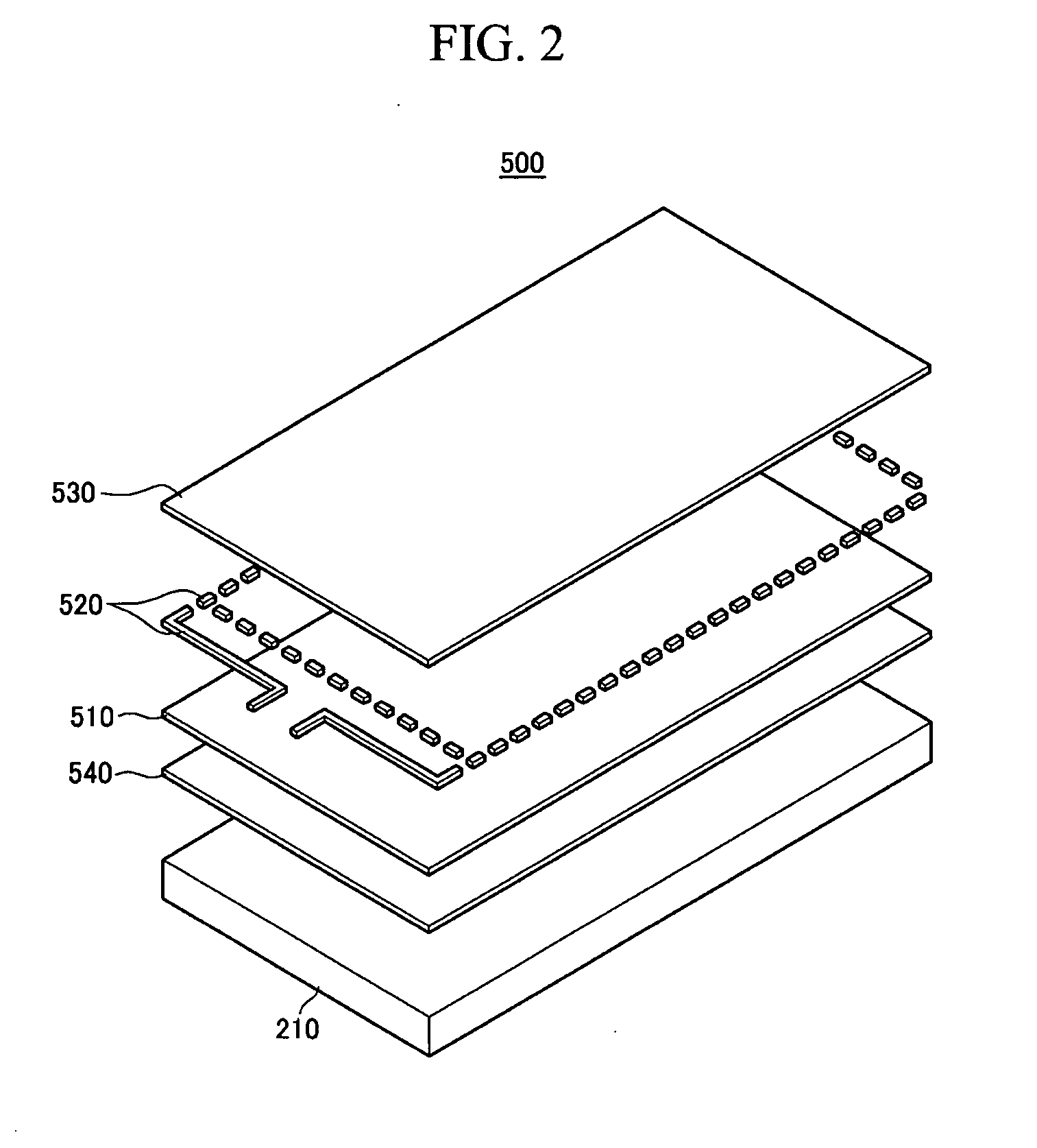
The present invention provides a panel assembly that can perform both an input function and a display function. The panel assembly includes two display panels and a touch sensing unit. The touch sensing unit includes an electrostatic induction insulating layer, an electrostatic induction pattern layer, and a dielectric layer. The first display panel includes thin film transistors, pixel electrodes, and a color filter. The second display panel includes a common electrode. An electromagnetic wave shield layer may be disposed between the electrostatic induction insulating layer and the second insulation substrate, and a polarization layer may be disposed between the color filter and the second insulation substrate. The panel assembly may further include a liquid crystal layer interposed between the first display panel and the second display panel.

Problems solved by technology

Therefore, in order to produce a display panel mounted with a touch panel, a problem may arise in that the overall manufacturing process may be complicated, and the productivity thereof is consequently lowered.
Further, in the related art, since the touch panel is separately manufactured and is then mounted on the display panel, a problem occurs in that the resolution of the display panel deteriorates due to the touch panel.
Furthermore, a problem occurs in that the image quality deteriorates due to degradation of optical characteristic of the touch panel.
Still further, since an additional touch panel is mounted on the display panel, a problem occurs in that the display area of the display panel is reduced.

Method used


Image

  • Panel assembly
  • Panel assembly
  • Panel assembly

Examples


Embodiment Construction

[0032]Hereinafter, a panel assembly according to the exemplary embodiments of the present invention will be described with reference to accompanying drawings. The exemplary embodiments of the present invention are for illustrative purposes and are not intended to limit the present invention. In the exemplary embodiments of the present invention, an LCD panel is used as a panel assembly, but the present invention is not limited thereto. That is, the present invention can be applied to flat display panels, such as a plasma display panel (PDP) and an organic light emitting display (OLED) panel. In addition, parts not related to the description may be omitted for clarity, and like reference numerals designate like elements and similar constituent elements throughout the specification. Constituent elements having the same configurations in the exemplary embodiments are exemplarily described in a first exemplary embodiment using like reference numerals, and configurations different from t...


PUM

PropertyMeasurementUnit
inclination angleaaaaaaaaaa
poweraaaaaaaaaa
transparentaaaaaaaaaa

Abstract

According to an embodiment of the present invention a panel assembly includes a first display panel having a first insulation substrate, a second display panel having a second insulation substrate opposite to the first insulation substrate, and a touch sensing unit formed on a surface of the second insulation substrate not facing the first insulation substrate. The touch sensing unit includes an electrostatic induction insulating layer formed on the second insulation substrate, an electrostatic induction pattern layer formed on the electrostatic induction insulating layer along edges of the electrostatic induction insulating layer, and a dielectric layer that covers the electrostatic induction insulating layer and the electrostatic induction pattern layer.

Description

CROSS-REFERENCE TO RELATED APPLICATION[0001]This application claims priority to and the benefit of Korean Patent Application No. 10-2006-0043732 filed in the Korean Intellectual Property Office on May 16, 2006, the entire contents of which are incorporated herein by reference.BACKGROUND OF THE INVENTION[0002](a) Field of the Invention[0003]The present invention relates to a panel assembly. More particularly, the present invention relates to a panel assembly having an input function.[0004](b) Description of the Related Art[0005]In recent years, the demand for display devices such as liquid crystal displays (LCDs) has exploded as these display devices have become smaller and lighter and have increased in performance due to rapidly advancing semiconductor technology. Since LCDs have various advantages, including they are small and light and have low power consumption, LCDs have been drawing attention as a substitute display device that can overcome many of the drawbacks of cathode ray ...

Claims


Application Information

Patent Timeline
Patent Type & Authority Applications(United States)
IPC IPC(8): G09G3/36G06F3/041G02F1/1335
CPCG06F3/044G02F1/13338G06F3/0445G02F1/1333
Inventor CHOO, DAE-HOKANG, HO-MIN
Owner SAMSUNG DISPLAY CO LTD
Learn More