IBIS correction tool, IBIS correction method, and waveform simulation device

Inactive Publication Date: 2007-08-09
FUJITSU LTD
View PDF3 Cites 13 Cited by
  • Summary
  • Abstract
  • Description
  • Claims
  • Application Information

AI Technical Summary

Benefits of technology

[0012]Accordingly, in consideration of the above-described problem, an object of the present invention is to provide an IBIS correction tool and an IBIS correction method able to generate corrected IBIS data corrected so as to match with any desired power supply voltage different from a specific power supply voltage in a short time and with a high precision based on the IBIS data for the specific power supply voltage and a waveform simulation device provided with this IBIS correction tool.

Problems solved by technology

This is because in recent semiconductor devices, the range of usable power supply voltage has grown greatly, so it has become difficult for the LSI manufacturer to provide the output voltage-current characteristic data under each power supply voltage over the entire range of the usable power supply voltage.
However, when performing the simple voltage shift explained above for the above correction, there is the problem that, in part of the above-described output voltage-current characteristic, there is a part which ends up deviating from the output voltage-current characteristic obtained by actual measurement or simulation.
Error occurs there, so corrected IBIS data corresponding to the above-described desired power supply voltage cannot be obtained with a high precision.
However, enormous time and cost are required for such actual measurement or simulation, so this is not realistic.

Method used


Image

  • IBIS correction tool, IBIS correction method, and waveform simulation device
  • IBIS correction tool, IBIS correction method, and waveform simulation device
  • IBIS correction tool, IBIS correction method, and waveform simulation device

Examples


Embodiment Construction

[0026]Preferred embodiments of the present invention will be described in detail below while referring to the attached figures.

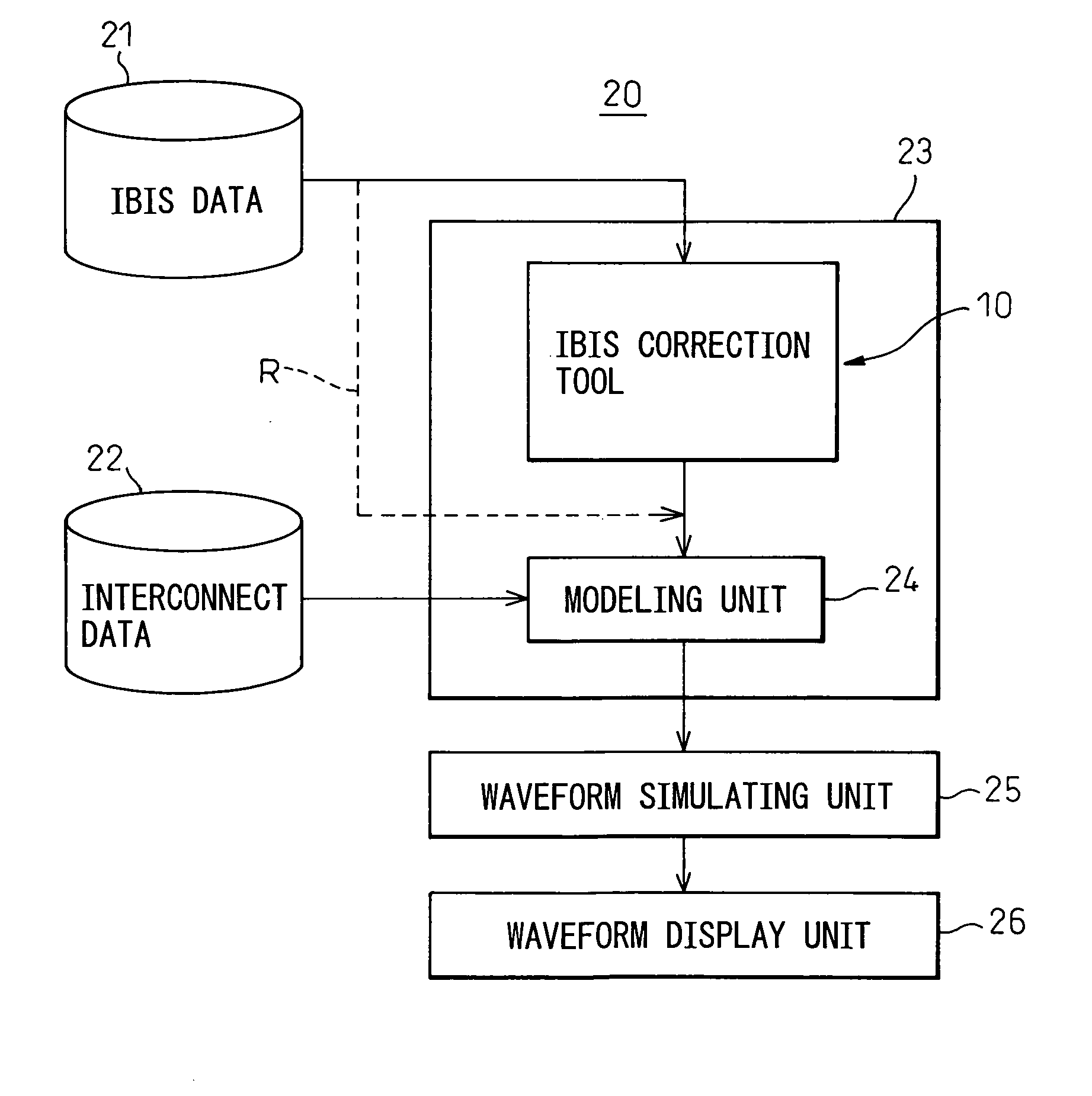
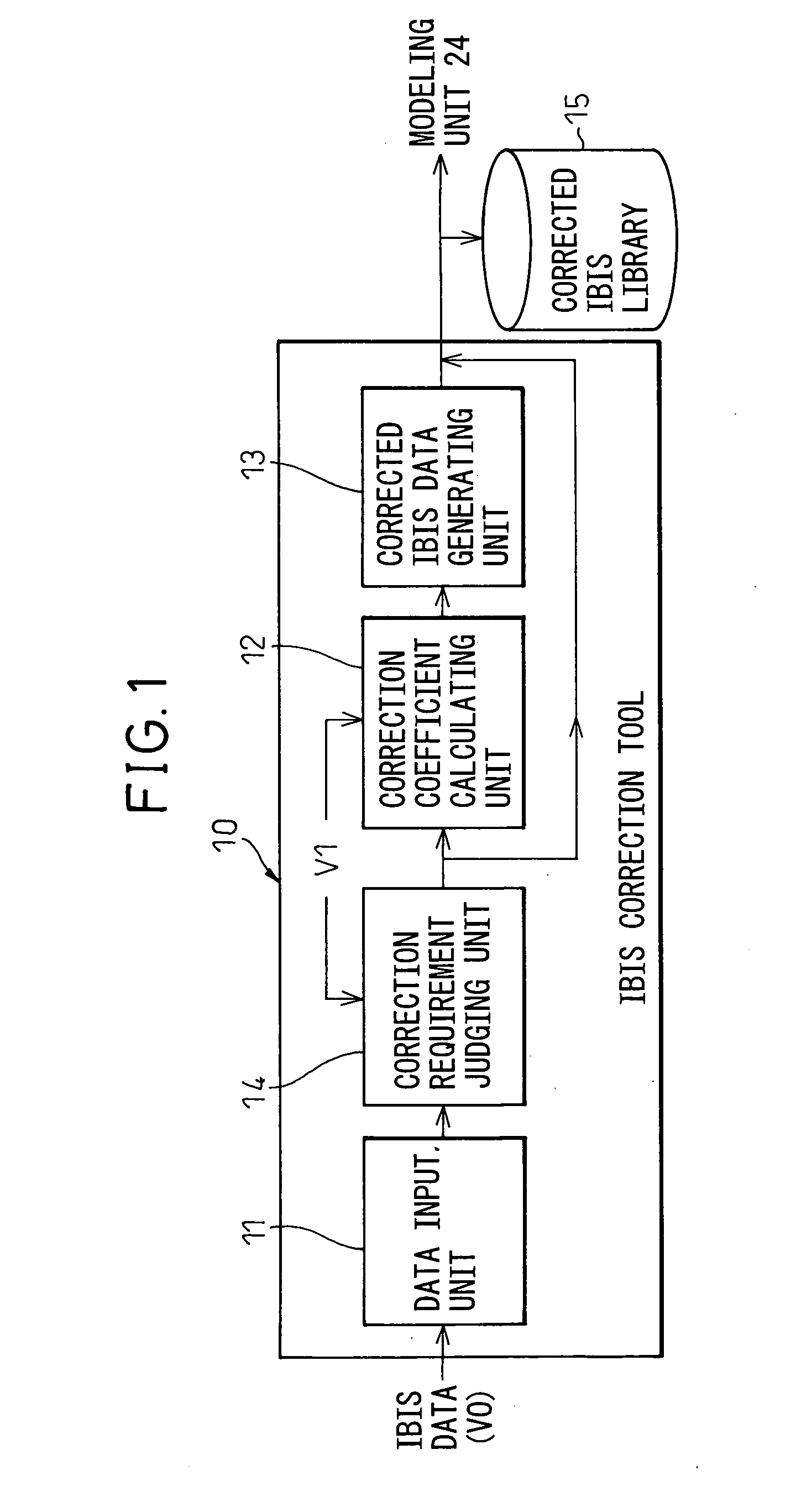
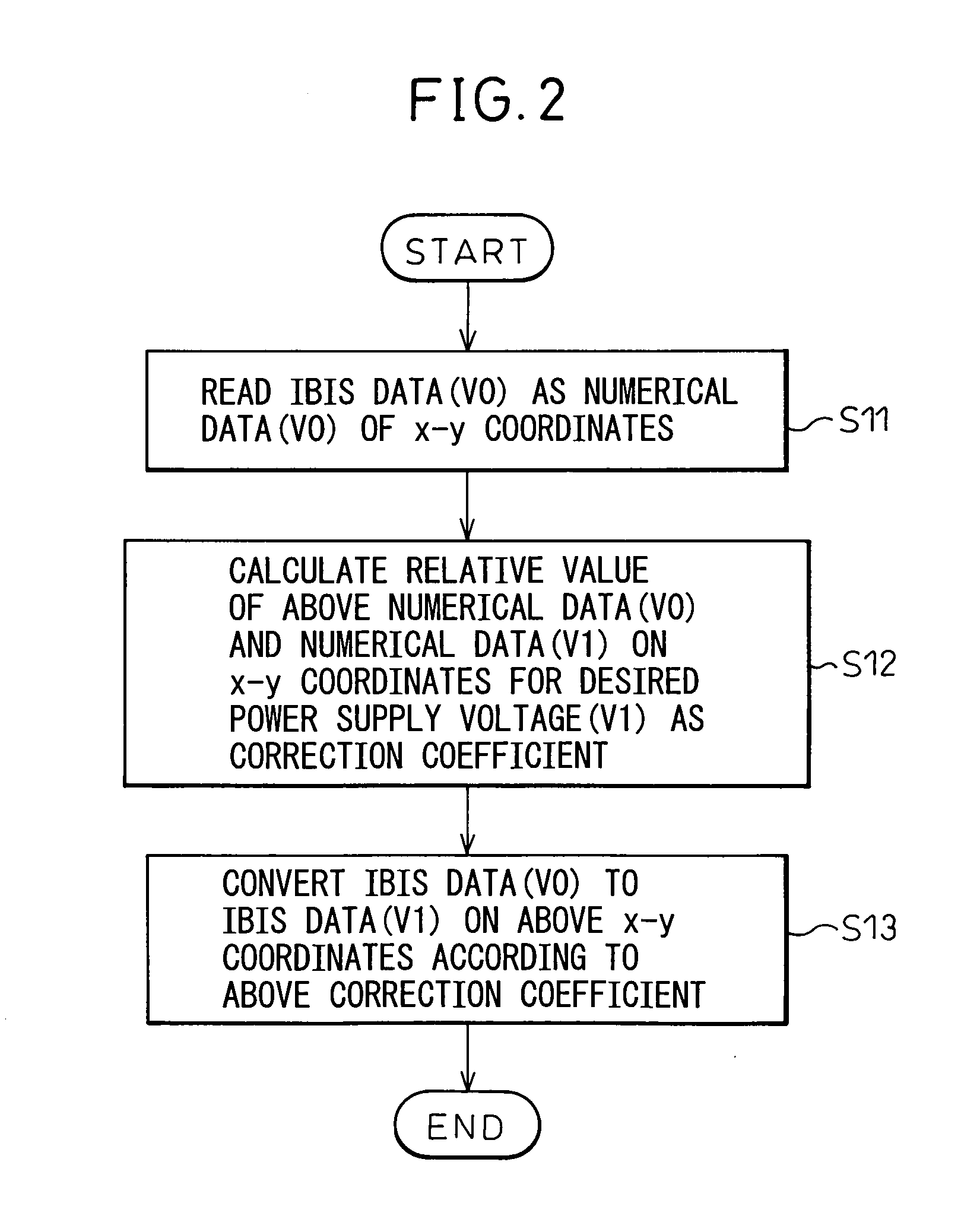
[0027]FIG. 1 is a diagram showing the basic configuration of an IBIS correction tool according to the present invention. In the figure, reference numeral 10 indicates an IBIS correction tool which is basically configured by illustrated data input unit 11, correction coefficient calculating unit 12, and corrected IBIS data generating unit 13. Note that, other than these, a correction requirement judging unit 14 and a corrected IBIS library 15 will be explained later.

[0028]This correction tool 10 is for converting IBIS data (V0) provided for a certain specific power supply voltage (for example V0) for a certain semiconductor device to corrected IBIS data corrected so as to match with a desired power supply voltage (for example V1) different from that specific power supply voltage for that semiconductor device. That IBIS data (V0) is input to the data input uni...


PUM


Abstract

An IBIS correction tool which can be used assembled in a waveform simulation device and corrects IBIS data for a certain specific power supply voltage V0 to IBIS data for a desired power supply voltage V1 with a higher precision than the past, that is, an IBIS correction tool configured so as to read IBIS data for a power supply voltage V0 as numerical data of x-y coordinates at a data input unit, find a relative ratio (correction coefficient) between this numerical data and numerical data for a power supply voltage V1 on its x-y coordinates at a correction coefficient calculating unit, and obtain corrected IBIS data corrected for the power supply voltage V1 according to that correction coefficient at a corrected IBIS data generating unit.

Description

BACKGROUND OF THE INVENTION[0001]1. Field of the Invention[0002]The present invention relates to, as one preferred example of application, a waveform simulation device for simulating an output waveform exhibited by a semiconductor device, more particularly relates to an input / output buffer information specification (IBIS) correction tool installed in the waveform simulation device etc. and an IBIS correction method.[0003]2. Description of the Related Art[0004]In recent years, LSIs and other semiconductor integrated circuits have been increasingly growing in circuit size. Simulators using computers are therefore becoming indispensable for their circuit design and circuit analysis. Among such simulators, the present invention particularly relates to a waveform simulation device for simulating the output waveforms of the basic components of semiconductor integrated circuits, that is, CMOS devices or other semiconductor devices as one preferred example of application. In further detail,...

Claims


Application Information

Patent Timeline
IPC IPC(8): G06F17/50
CPCG06F17/5036G06F30/367
Inventor SUWA, YUJIYONEDA, JIRO
Owner FUJITSU LTD
Why Eureka
Try Eureka