Storage controller
- Summary
- Abstract
- Description
- Claims
- Application Information
AI Technical Summary
Benefits of technology
Problems solved by technology
Method used
Image

Examples
embodiment 1
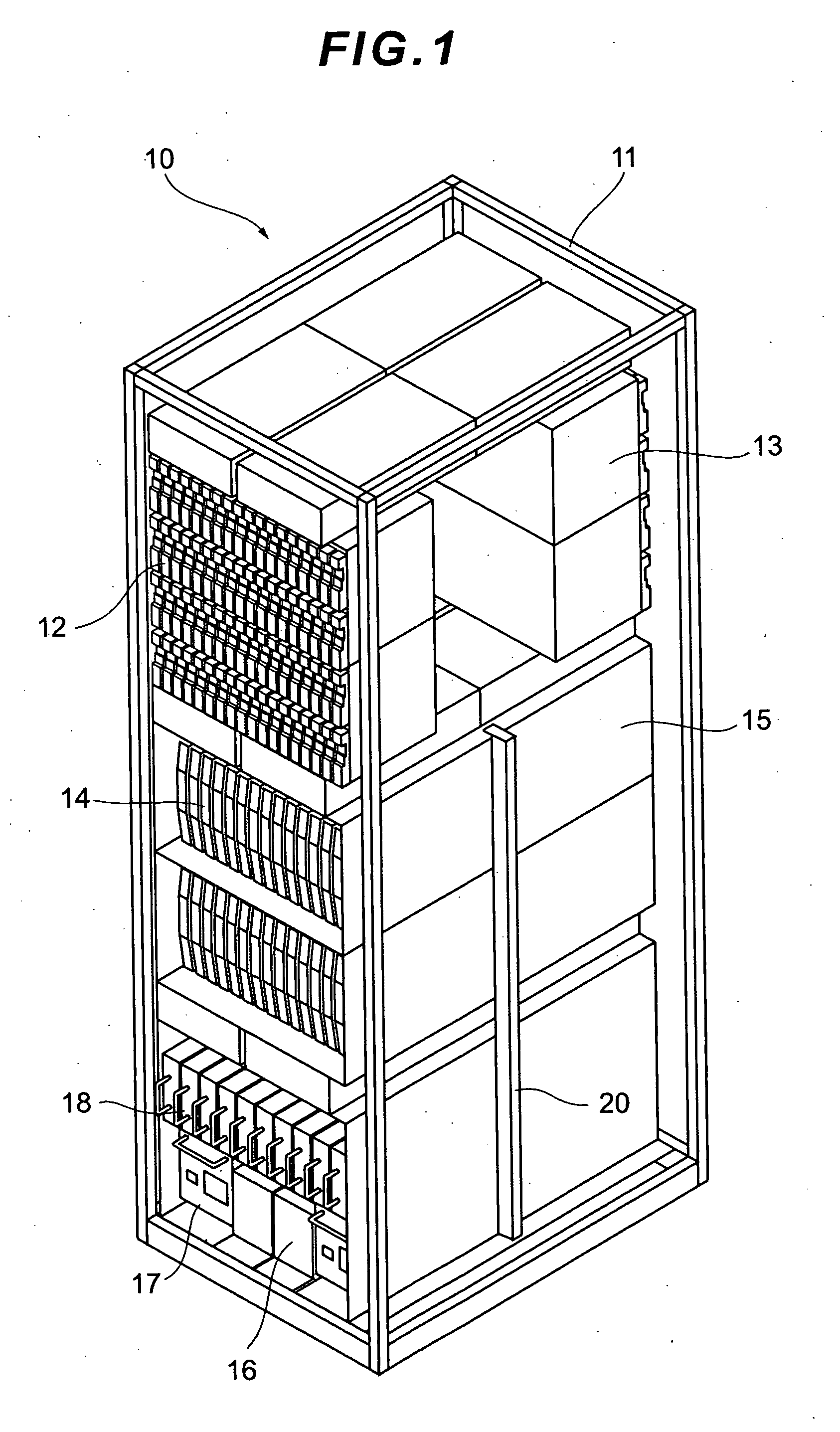
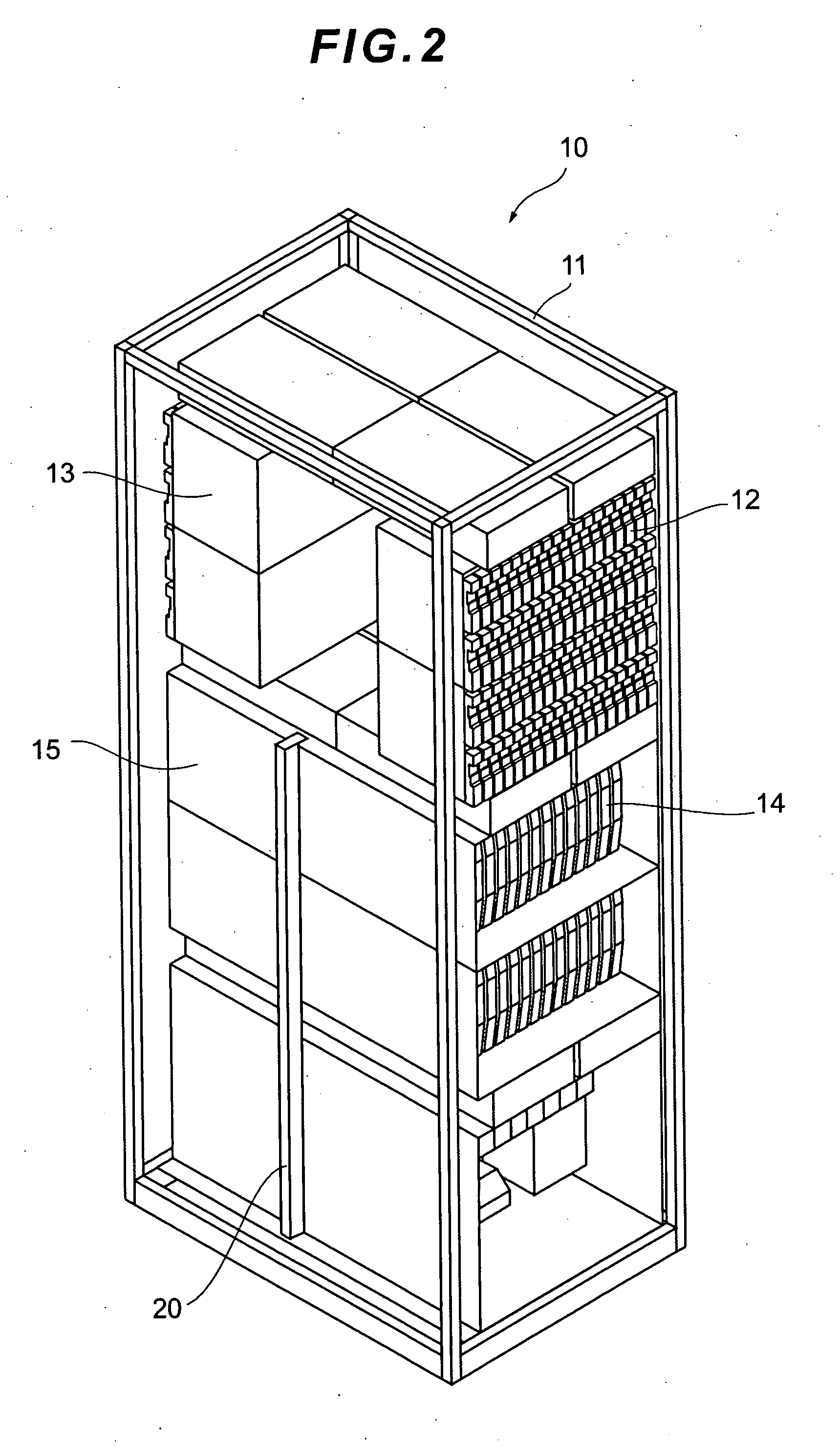
[0025]FIG. 1 is a front perspective view of a disk array system 10 according to the present invention and FIG. 2 is a rear perspective view of the disk array system 10. As shown in the drawings, the disk array system 10 has a basic frame 11, disk boxes 13, logical board boxes 15, and alternating-current power sources 16.
[0026] The basic frame 11 has a rack-shaped frame structure, in which the disk boxes 13, logical board boxes 15, and alternating-current power sources 16 are mounted.
[0027] A disk box 13 has a box structure for mounting a plurality of disk drives 12 therein. Examples of the disk drives 12 include Fibre Channel (FC) disk drives, Serial Advanced Technology Attachment (SATA) disk drives, Parallel Advanced Technology Attachment (PATA) disk drives, Fibre Attached Technology Adapted (FATA) disk drives, and Small Computer System Interface (SCSI) disk drives.
[0028] A logical board box 15 is for mounting a plurality of logical boards 14. The logical boards 14 are controlle...
embodiment 2
[0039] Embodiment 2 is explained with reference to FIG. 9 to FIG. 12. FIG. 9 shows another connector structure for the logical board 14. FIG. 10 shows the connection structure of the logical boards 14 and the surface layer 21. As shown in the drawings, the signal connector 141 and the power source connector 142 are formed on the backplane connection side of the logical board 14 and ports P0 to P3 are formed on the host interface connection side. The power source connector 142 is formed on one end of the backplane connection side. The ports P0 to P3 connect with the host interfaces. 14A indicates a front face of the logical board 14 and 14B indicates a back face of the logical board 14. When the logical board 14 is mounted on the upper level of the surface layer 21, the power source connector 142 is connected to the power source connector 210A and the signal connector 141 is connected to the signal connector 211A. Meanwhile, when the logical board 14 is mounted on the lower level of ...
embodiment 3
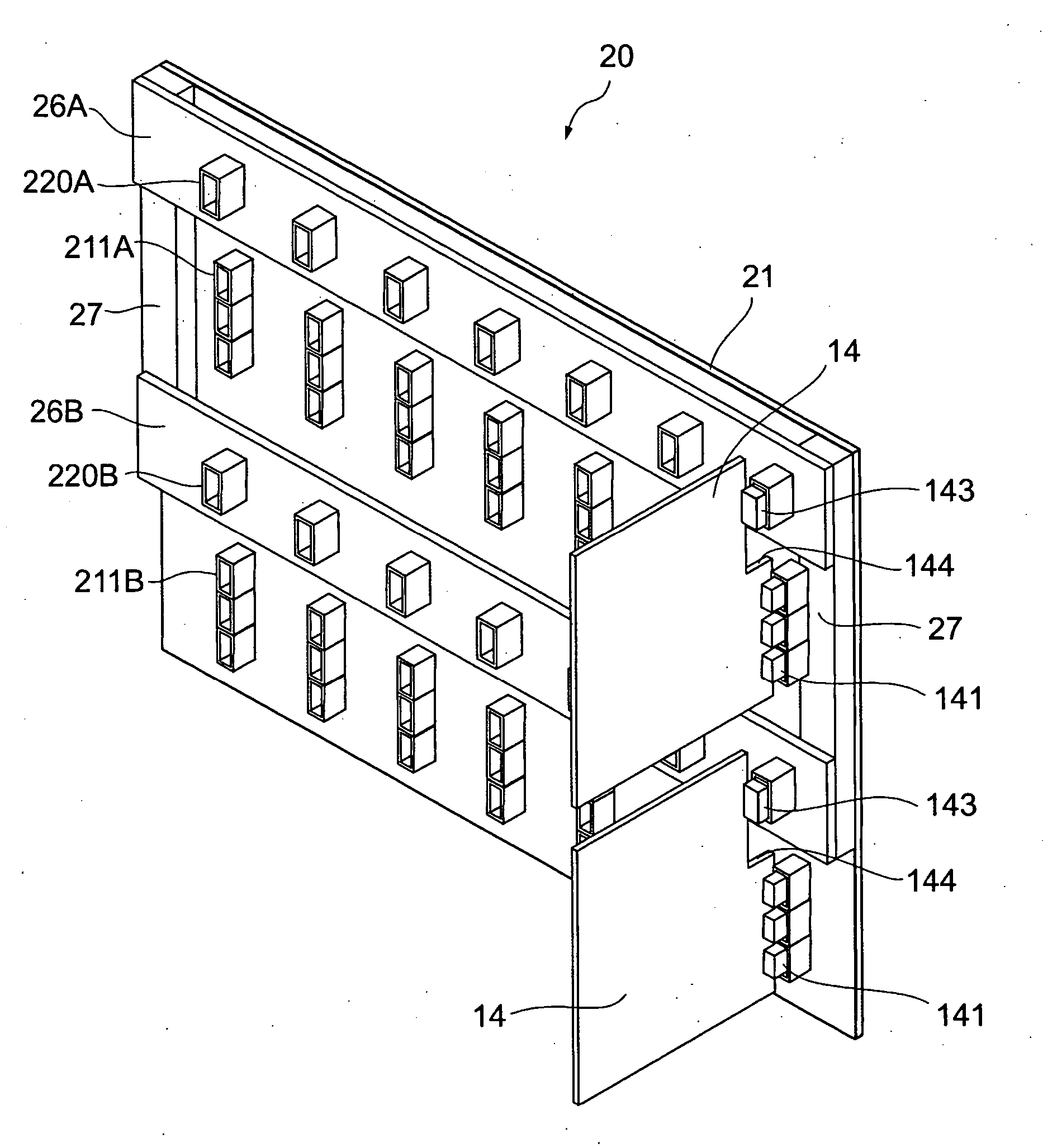
[0045] Embodiment 3 is explained with reference to FIG. 13 and FIG. 14. Components having the same reference numbers as in FIG. 3 indicate the same components, therefore detailed explanations thereof are omitted. As shown in FIG. 13, power source plates 26A and 26B are formed over the surface layer 21 via supporting elements 27. The power source plate 26A has a plurality of power source connectors 220A and is formed at the top end side of the backplane 20. The power source plate 26B has a plurality of power source connectors 220B and is formed crossing substantially the center of the backplane 20. Both the power source plates 26A and 26B are bridged over and are a certain distance (distance corresponding to the thickness of the supporting elements 27) away from the surface layer 21. The power source plates 26A and 26B are conductive plates for supplying power to the power source connectors 220A and 220B. The supporting elements 27 are made of a conductive material and function as bu...
PUM
 Abstract
Description
Claims
Application Information
 - R&D
- Intellectual Property
- Life Sciences
- Materials
- Tech Scout
- Unparalleled Data Quality
- Higher Quality Content
- 60% Fewer Hallucinations
Browse by: Latest US Patents, China's latest patents, Technical Efficacy Thesaurus, Application Domain, Technology Topic, Popular Technical Reports.
© 2025 PatSnap. All rights reserved.Legal|Privacy policy|Modern Slavery Act Transparency Statement|Sitemap|About US| Contact US: help@patsnap.com