Optical module
a technology of optical modules and optical light guides, applied in the field of optical modules, can solve the problems of interference between semiconductor lasers and cannot be prevented, and achieve the effect of improving the efficiency of optical modules
- Summary
- Abstract
- Description
- Claims
- Application Information
AI Technical Summary
Benefits of technology
Problems solved by technology
Method used
Image


Examples
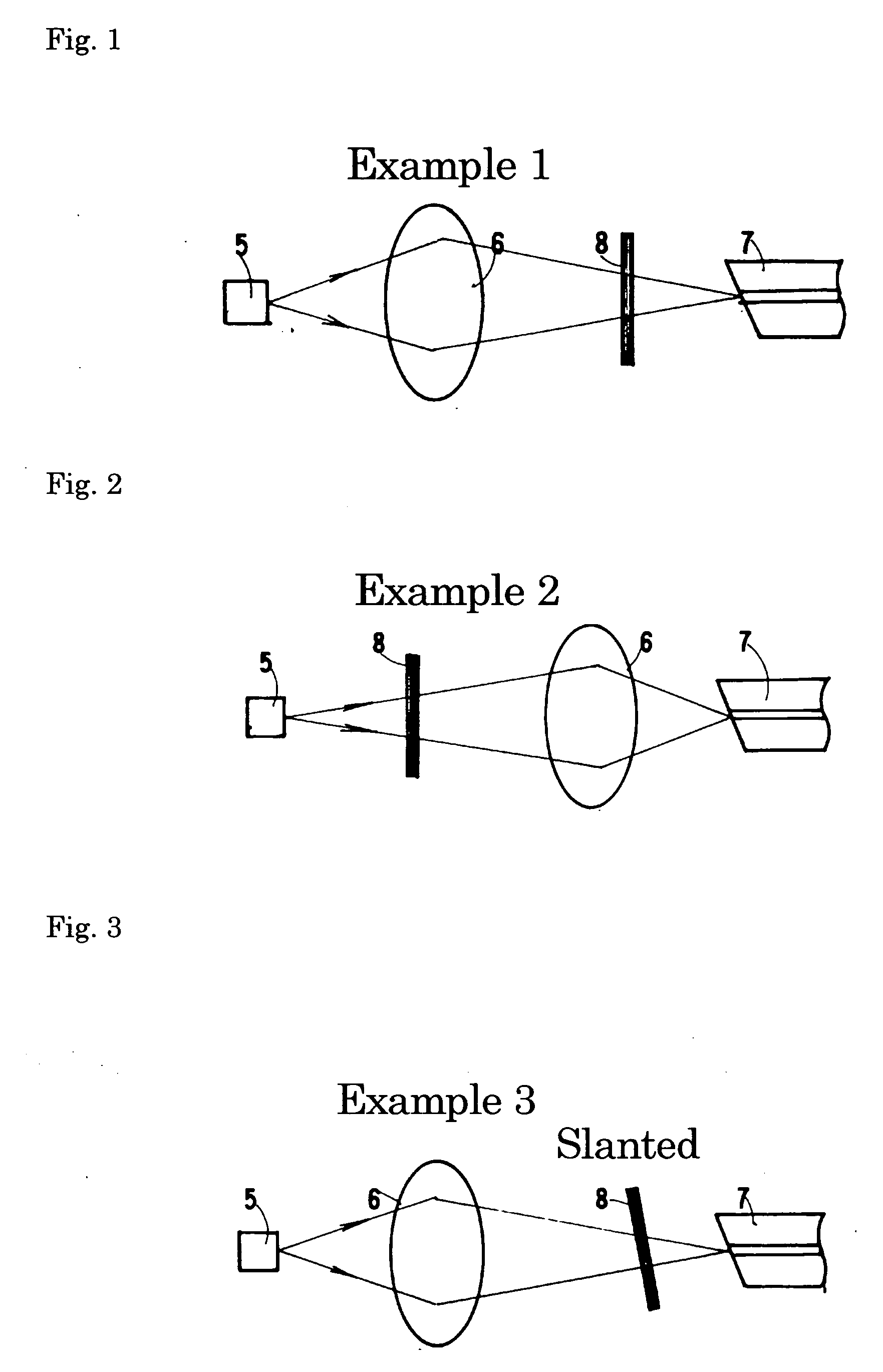
example 1
FIG. 1: LD+Lens+Filter+Optical Fiber
[0096]FIG. 1 shows Example 1. A lens 6 and an optical fiber 7 are placed on the light-outgoing-side optical axis of a semiconductor laser (LD) 5. Between the lens 6 and the optical fiber 7, a natural emission lightwave-blocking filter 8 is placed that blocks a natural emission lightwave of the semiconductor laser (LD) 5. The lightwave of the semiconductor laser (LD) 5 is condensed by the lens 6 to be focused on the end face of the optical fiber. The semiconductor laser (LD) 5 generates not only a laser oscillation lightwave having an intended wavelength of Λq but also a natural emission lightwave Σn having different wavelengths. Nevertheless, the natural emission lightwave-blocking filter 8 blocks the natural emission lightwave Σn, transmitting only the laser oscillation lightwave Λq. As a result, only the laser oscillation lightwave Λq enters the optical fiber 7. When the natural emission lightwave-blocking filter is placed between the lens and ...
example 2
FIG. 2: LD+Filter+Lens+Optical Fiber
[0097]FIG. 2 shows Example 2. A lens 6 and an optical fiber 7 are placed on the light-outgoing-side optical axis of a semiconductor laser (LD) 5. Between the semiconductor laser (LD) 5 and the lens 6, a natural emission lightwave-blocking filter 8 is placed that blocks a natural emission lightwave of the semiconductor laser (LD) 5. The semiconductor laser (LD) 5 generates not only a laser oscillation lightwave having an intended wavelength of Λq but also a natural emission lightwave Σn having different wavelengths. Nevertheless, the natural emission lightwave-blocking filter 8 blocks the natural emission lightwave Σn, transmitting only the laser oscillation lightwave Λq. As a result, only the laser oscillation lightwave enters the optical fiber 7. When the natural emission lightwave-blocking filter is placed between the LD and the lens, they can be hermetically sealed as a unitary body, enabling the miniaturization of the module.
example 3
FIG. 3: LD+Lens+Filter+Optical Fiber
[0098]FIG. 3 shows Example 3. A lens 6, a natural emission lightwave-blocking filter 8, and an optical fiber 7 are placed in this order on the light-outgoing-side optical axis of a semiconductor laser (LD) 5. The filter 8 is slanted in order to eliminate the feedback lightwave to the semiconductor laser due to the reflection from the filter 8. The natural emission lightwave-blocking filter 8 blocks the natural emission lightwave Σn included in the lightwave of the semiconductor laser (LD) 5, introducing only the laser oscillation lightwave Λq into the optical fiber 7.
PUM
 Abstract
Description
Claims
Application Information
 - R&D
- Intellectual Property
- Life Sciences
- Materials
- Tech Scout
- Unparalleled Data Quality
- Higher Quality Content
- 60% Fewer Hallucinations
Browse by: Latest US Patents, China's latest patents, Technical Efficacy Thesaurus, Application Domain, Technology Topic, Popular Technical Reports.
© 2025 PatSnap. All rights reserved.Legal|Privacy policy|Modern Slavery Act Transparency Statement|Sitemap|About US| Contact US: help@patsnap.com