
Self-packaged optical interference display device having anti-stiction bumps, integral micro-lens, and reflection-absorbing layers

a display device and self-packaging technology, applied in static indicating devices, liquid/fluent solid measurements, instruments, etc., can solve the problems of increasing weight and cost, power usage, and the size of the battery contained, and achieve the effect of reducing undesired reflections

Inactive Publication Date: 2007-01-25
PIEHL ARTHUR +3
View PDF6 Cites 142 Cited by
  • Summary
  • Abstract
  • Description
  • Claims
  • Application Information

AI Technical Summary

Benefits of technology

The invention is an electronic device that can display pixels of a display image. It includes a cavity between two reflectors that can be adjusted to select the visible wavelength and intensity of the image. The device also has transparent films, absorbing layers, a micro-lens, and anti-stiction bumps. The films are for self-packaging, the absorbing layers reduce reflections, and the micro-lens focuses the image. The anti-stiction bumps prevent the reflectors from sticking together. Overall, the device can display pixels of a display image with high precision and clarity.

Problems solved by technology

Since power must continually be supplied to these types of displays, they can be a significant cause of power usage in devices where supplied power is at a premium, such as portable devices like laptop and notebook computers, personal digital assistant (PDA) devices, wireless phones, as well as other types of portable devices.
As a result, designers of such devices usually choose to increase the size of the battery size contained in such devices, increasing weight and cost, or choose to reduce the running time of the devices between battery charges.

Method used


Image

  • Self-packaged optical interference display device having anti-stiction bumps, integral micro-lens, and reflection-absorbing layers
  • Self-packaged optical interference display device having anti-stiction bumps, integral micro-lens, and reflection-absorbing layers
  • Self-packaged optical interference display device having anti-stiction bumps, integral micro-lens, and reflection-absorbing layers

Examples


Embodiment Construction

[0018] In the following detailed description of exemplary embodiments of the invention, reference is made to the accompanying drawings that form a part hereof and in which is shown by way of illustration specific exemplary embodiments in which the invention may be practiced. These embodiments are described in sufficient detail to enable those skilled in the art to practice the invention. Other embodiments may be utilized, and logical, mechanical, and other changes may be made without departing from the spirit or scope of the present invention. The following detailed description is, therefore, not to be taken in a limiting sense, and the scope of the present invention is defined only by the appended claims.

Overview

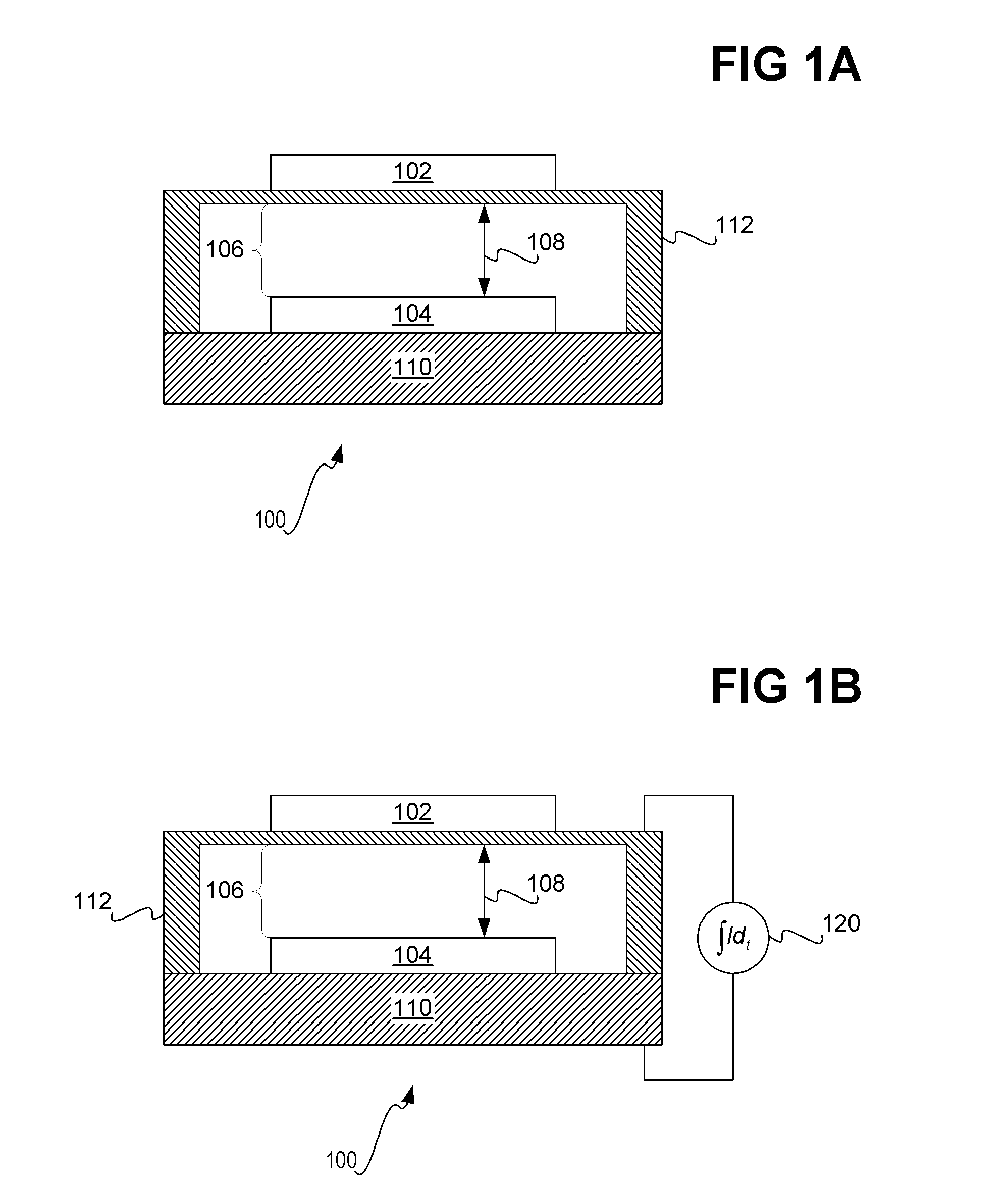
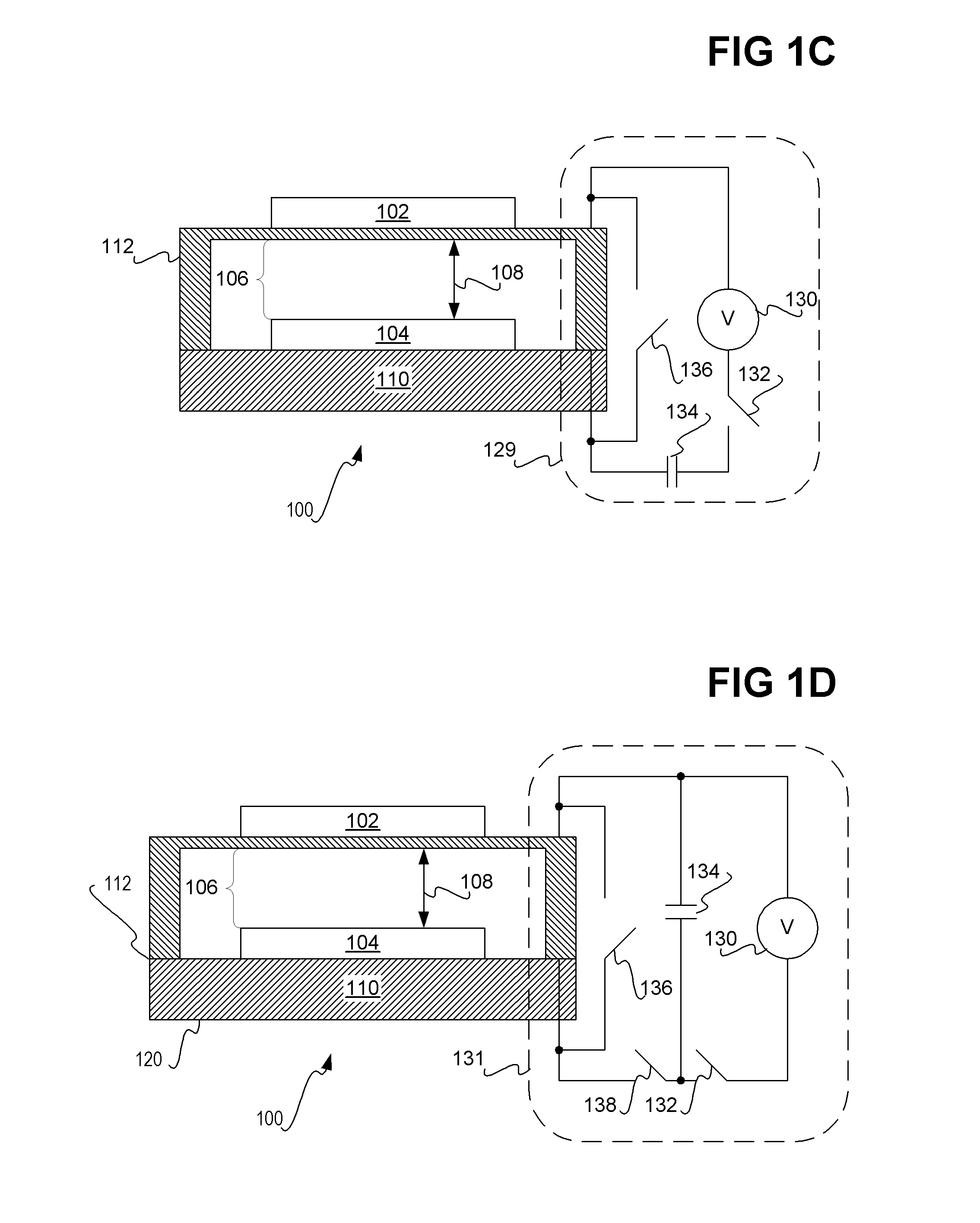
[0019]FIG. 1A shows an electronic device 100 for at least partially displaying a pixel of a displayable image, according to an embodiment of the invention. The device 100 includes a top reflector 102 and a bottom reflector 104, as well as a flexure 110 and a spring mecha...


PUM

PropertyMeasurementUnit
blue wavelengthaaaaaaaaaa
electrostatic forceaaaaaaaaaa
thicknessaaaaaaaaaa

Abstract

An electronic device of an embodiment of the invention is disclosed that at least partially displays a pixel of a display image. The device includes a first reflector and a second reflector defining an optical cavity therebetween that is selective of a visible wavelength at an intensity. The device includes a mechanism to allow optical properties of the cavity to be varied such that the visible wavelength and / or the intensity are variably selectable in correspondence with the pixel of the displayable image. The device also includes one or more transparent deposited films, one or more absorbing layers, an integral micro-lens, and / or one or more anti-stiction bumps. The deposited films are over one of the reflectors, for self-packaging of the device. The absorbing layers are over one of the reflectors, to reduce undesired reflections. The integral micro-lens is over one of the reflectors, and the anti-stiction bumps are between the reflectors.

Description

BACKGROUND [0001] Nearly all conventional displays are active in nature. This means that power must continually be supplied to the displays for them to maintain the images they are displaying. Such conventional displays include direct view and projection cathode-ray tube (CRT) displays, direct view and projection liquid crystal displays (LCD's), direct view plasma displays, projection digital light processing (DLP) displays, and direct view electroluminescent (EL) displays, among others. [0002] Since power must continually be supplied to these types of displays, they can be a significant cause of power usage in devices where supplied power is at a premium, such as portable devices like laptop and notebook computers, personal digital assistant (PDA) devices, wireless phones, as well as other types of portable devices. As a result, designers of such devices usually choose to increase the size of the battery size contained in such devices, increasing weight and cost, or choose to reduc...

Claims


Application Information

Patent Timeline
Patent Type & Authority Applications(United States)
IPC IPC(8): H01L21/31H01L21/469B81B3/00G02B1/11G02B26/00G09G3/34
CPCB81B3/0008B81B2201/047G09G2300/06G02B26/001G09G3/3466G02B1/11
Inventor PIEHL, ARTHURPRZYBYLA, JAMES R.GHOZEIL, ADAM L.MARTIN, ERIC T.
Owner PIEHL ARTHUR
Learn More