
Display device and driving method of display device

a display device and driving method technology, applied in the direction of electric digital data processing, instruments, computing, etc., can solve the problem of difficult to expect further substantial reduction of the transfer rate, and achieve the effect of uniform transfer rate and reduced display data transfer ra

Inactive Publication Date: 2007-01-04
SONY CORP
View PDF4 Cites 11 Cited by
  • Summary
  • Abstract
  • Description
  • Claims
  • Application Information

AI Technical Summary

Benefits of technology

[0012] It is accordingly desirable to provide a display device and a driving method of the display device that can greatly reduce the transfer rate of display data.
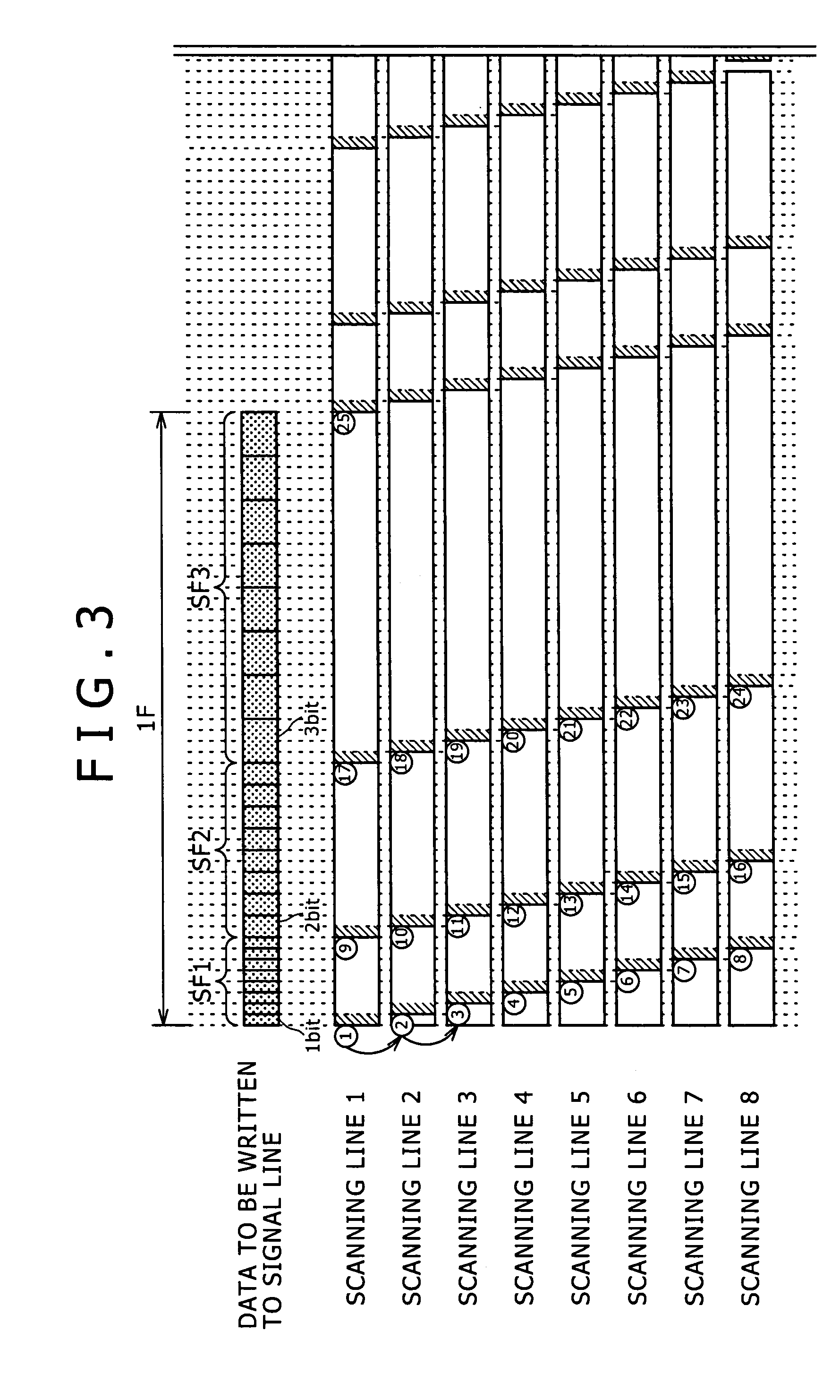
[0015] According to an embodiment of the present invention, it is possible to transfer the display data at a uniform transfer rate and thus greatly reduce the transfer rate of the display data. In addition, since the sampling time is constant without depending on bits, the number of gradation levels is not limited by the transfer rate of minimum bits.

Problems solved by technology

However, while the related technique can reduce the transfer rate of the display data transferred to the display device to ½ because the subfields are sorted into the two groups for the odd-numbered lines and the even-numbered lines, a further substantial reduction of the transfer rate is difficult to be expected.

Method used


Image

  • Display device and driving method of display device
  • Display device and driving method of display device
  • Display device and driving method of display device

Examples


Embodiment Construction

[0028] A preferred embodiment of the present invention will hereinafter be described in detail with reference to the drawings.

[0029]FIG. 5 is a block diagram showing an outline of a configuration of a display device according to an embodiment of the present invention. Description in the following will be made by taking, as an example of the display device, a digital driving active matrix type liquid crystal display device that uses a liquid crystal cell as an electrooptic element of a pixel and makes gradation display by pulse width modulation (PWM).

[0030] The active matrix type liquid crystal display device 10 according to the present embodiment includes a pixel array unit 11, a vertical driving circuit 12, and a horizontal driving circuit 13. These circuits are integrated on a same substrate (hereinafter referred to as a liquid crystal panel 14) as the pixel array unit 11.

[0031] The pixel array unit 11 is formed such that pixels 20 including a liquid crystal cell as an electroo...


PUM


Abstract

A digital driving display device to make gradation display by pulse width modulation includes: a pixel array unit arranging pixels having an electrooptic element and incorporating a memory in a matrix, disposing a scanning line for each row in a pixel arrangement in the matrix, and a signal line for each column; a horizontal driving section inputting display data in a block for each scanning line having a low to a high gradation level subfield for each bit of the data defining gradation levels of the pixels and in a period for weight of the bit, sampling-latching, sequentially transferring, and supplying the data to the signal line; and a vertical driving section selecting and scanning pixels of the pixel array unit in a row and performing scanning while jumping rows to write the data supplied in the block from the horizontal driving section to pixels of the pixel array unit.

Description

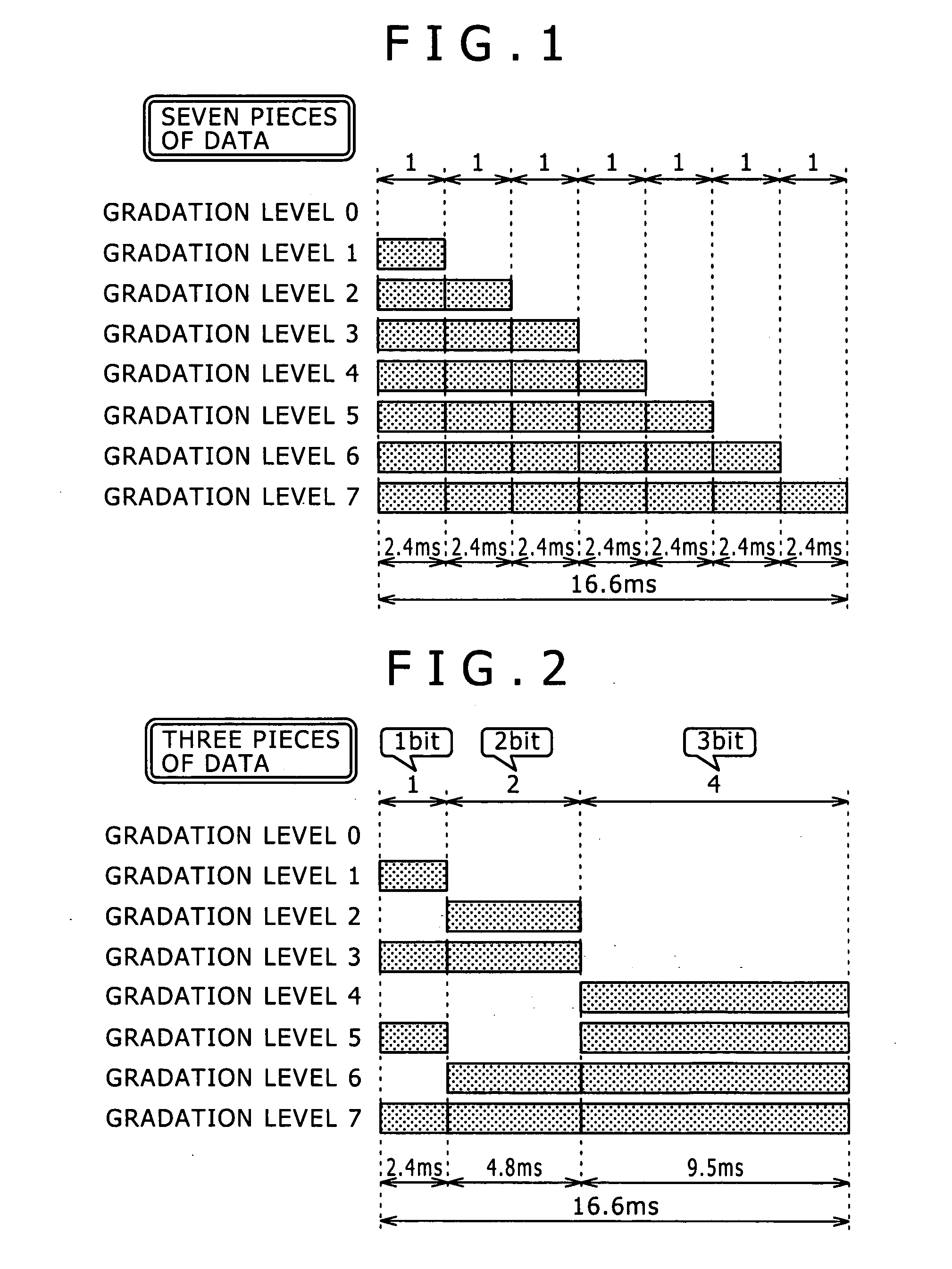
CROSS REFERENCES TO RELATED APPLICATIONS [0001] The present invention contains subject matter related to Japanese Patent Application JP 2005-170308 filed with the Japanese Patent Office on Jun. 10, 2005, the entire contents of which being incorporated herein by reference. BACKGROUND OF THE INVENTION [0002] 1. Field of the Invention [0003] The present invention relates to a display device and a driving method of the display device, and particularly to a digital driving display device that makes gradation display by pulse width modulation, and a driving method of the display device. [0004] 2. Description of Related Art [0005] When a case of three bits (eight gradation levels) is taken as an example, as shown in FIG. 1, a digital driving display device that makes gradation display by pulse width modulation (PWM) ideally uses a gradation display method for displaying eight gradation levels by setting a one-bit data of a 2.4 ms width, for example, as a unit and combining pieces of such u...

Claims


Application Information

Patent Timeline
Patent Type & Authority Applications(United States)
IPC IPC(8): G09G5/10
CPCG09G3/2014G09G3/3648G09G3/3688G09G2310/0227G09G2300/0842G09G2300/0857G09G2300/0809G09G3/20G09G3/30G09G3/36
Inventor SAKURAI, HIROYUKI
Owner SONY CORP
Learn More