Liquid crystal display device
a liquid crystal display and display device technology, applied in non-linear optics, instruments, optics, etc., can solve the problems of sacrificing front brightness, complicated manufacturing process, and affecting the quality of liquid crystal display devices, so as to achieve wider visibility, higher contrast, and wider visibility angle
- Summary
- Abstract
- Description
- Claims
- Application Information
AI Technical Summary
Benefits of technology
Problems solved by technology
Method used
Image
Examples
first embodiment
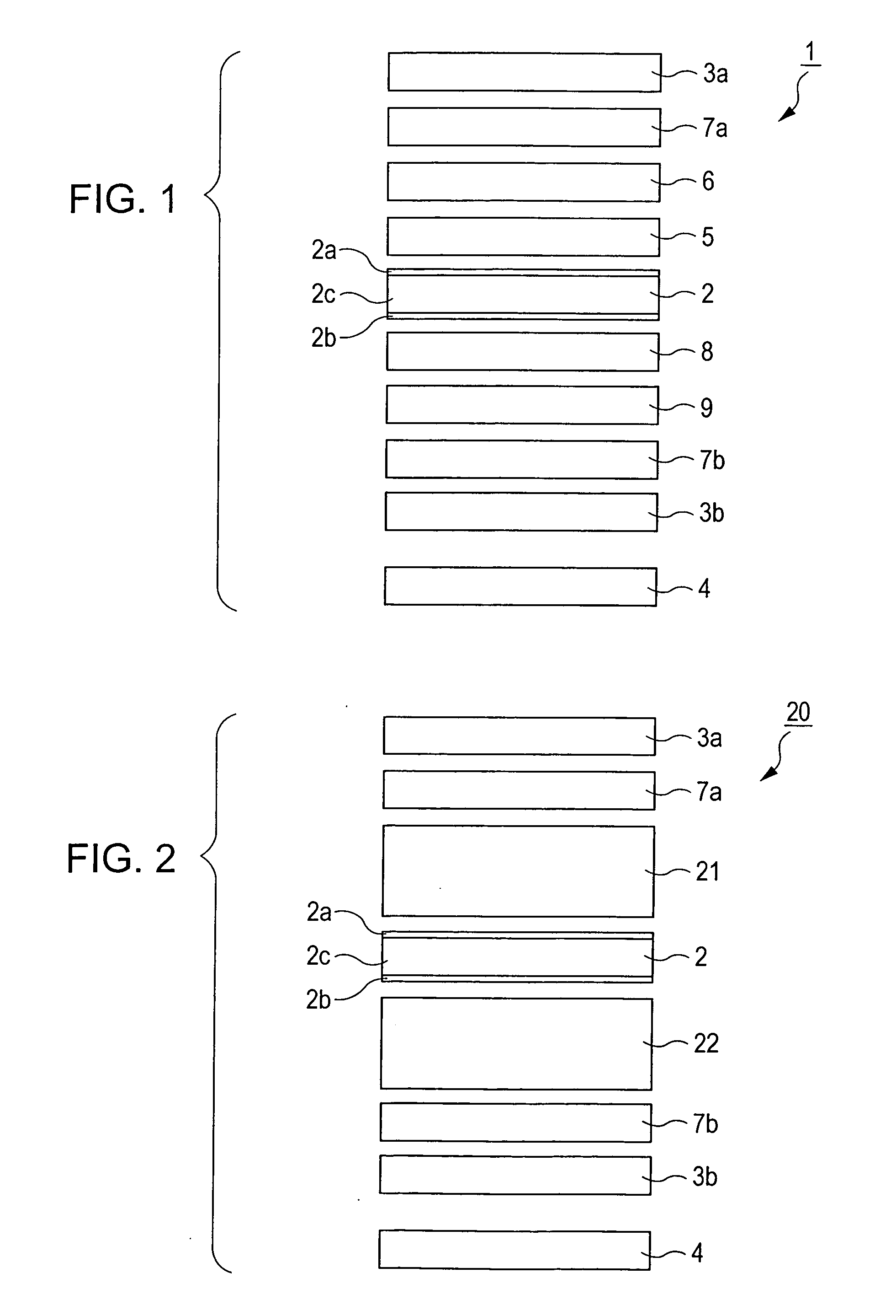
[0048] Firstly, a transflective liquid crystal display device 1 shown in FIG. 1 will be described as a first embodiment of the present invention. The transflective liquid crystal display device 1, shown in FIG. 1, includes a liquid crystal panel 2, polarizing plates 3a, 3b arranged on the front side and the back surface side of the liquid crystal panel 2, and a back light 4 arranged on the side of the polarizing plate 3b on the back side opposite from the liquid crystal panel 2.
[0049] The liquid crystal panel 2 includes a transparent substrate 2a formed with a transparent electrode and an alignment film that covers the transparent electrode formed on one main surface thereof, an active matrix substrate 2b arranged so as to oppose to the transparent substrate 2a and formed with a plurality of switching elements and pixel electrodes corresponding to the respective pixels and an alignment film that covers the plurality of pixel electrodes on a main surface opposing to the transparent ...
second embodiment
[0060] Subsequently, a transflective liquid crystal display device 20 shown in FIG. 2 will be described as a second embodiment of the present invention. In the following description, similar parts to the transflective liquid crystal display device 1 shown in FIG. 1 will not be described, and are represented by the same reference numerals.
[0061] The transflective liquid crystal display device 20 includes a fifth optical compensation plate 21 and the quarter-wave plate 7a in sequence from the side of the liquid crystal panel 2 between the liquid crystal panel 2 and the polarizing plate 3a on the front side, and a sixth optical compensation plate 22 and the quarter-wave plate 7b in sequence from the side of the liquid crystal panel 2 between the liquid crystal 2 and the polarizing plate 3b on the back surface side instead of the first to fourth optical compensation plates 5, 6, 8, 9 of the transflective liquid crystal display device 1. In other words, the transflective liquid crystal ...
third embodiment
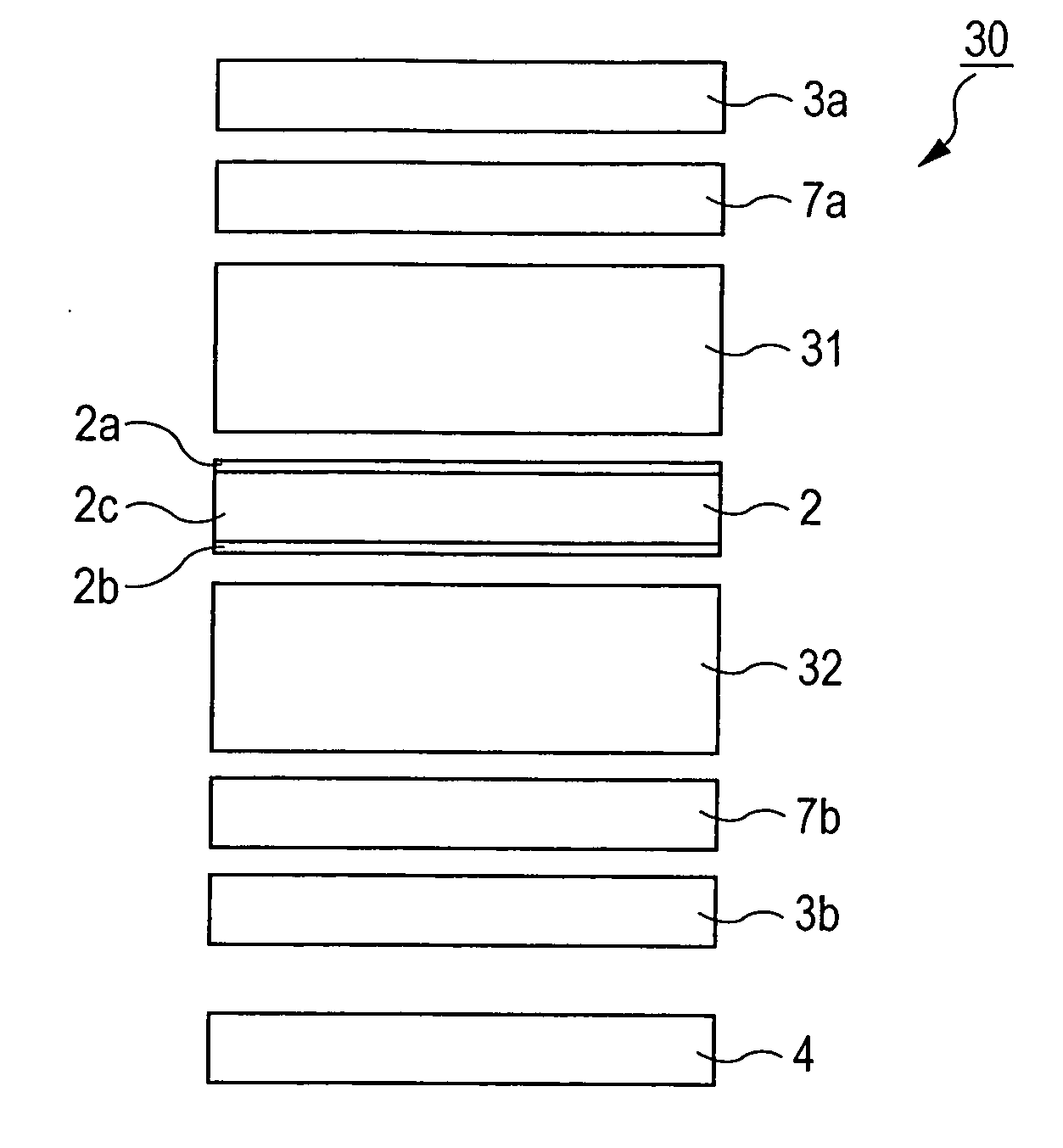
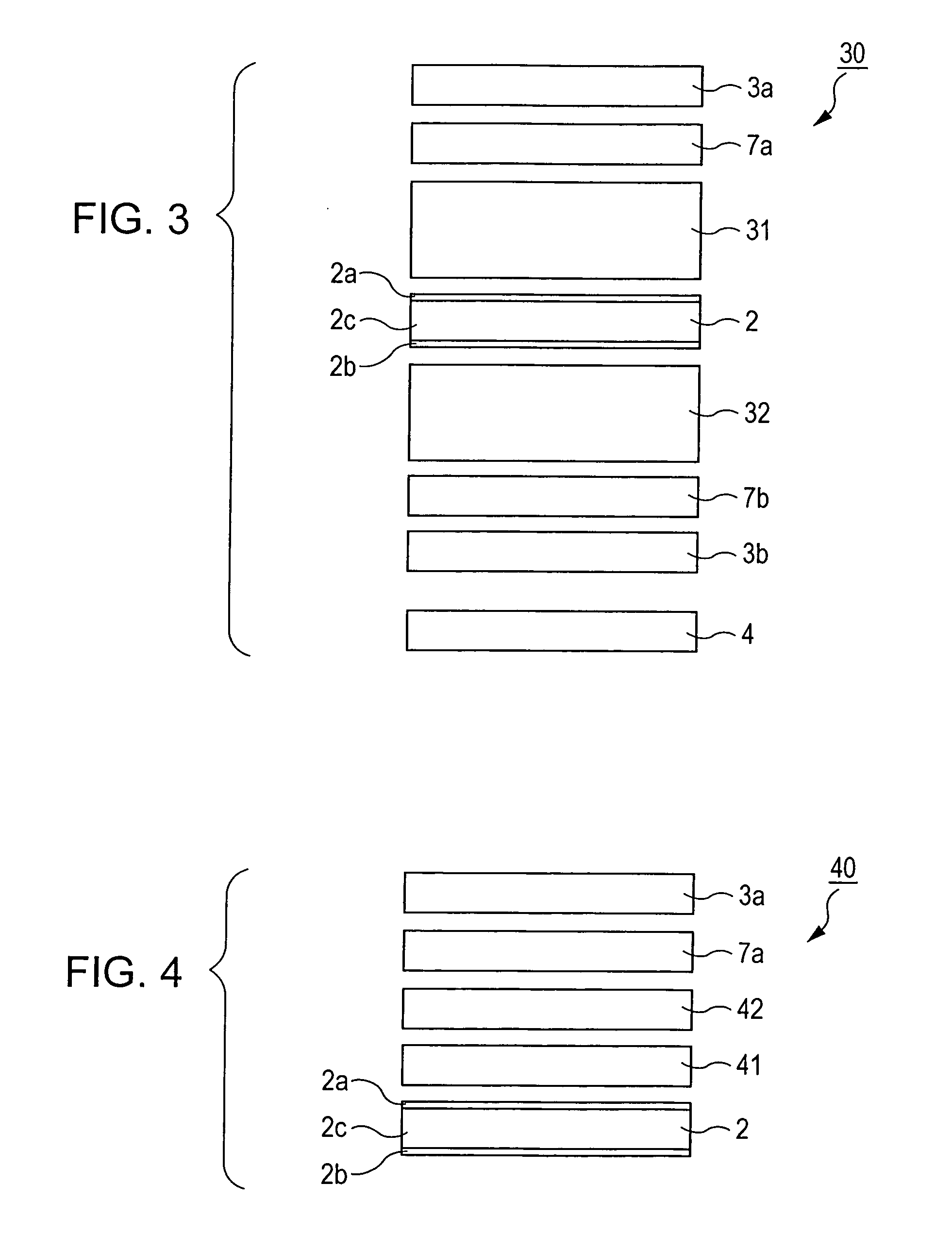
[0069] Subsequently, a transflective liquid crystal display device 30 shown in FIG. 3 will be described as a third embodiment of the present invention. In the following description, similar parts to the transflective liquid crystal display device 1 shown in FIG. 1 will not be described, and are represented by the same reference numerals.
[0070] The transflective liquid crystal display device 30 includes the seventh optical compensation plate 31 and the quarter-wave plate 7a in sequence from the side of the liquid crystal panel 2 between the liquid crystal panel 2 and the polarizing plate 3a on the front side, and an eighth optical compensation plate 32 and the quarter-wave plate 7b in sequence from the side of the liquid crystal panel 2 between the liquid crystal 2 and the polarizing plate 3b on the back surface side instead of the fifth and sixth optical compensation plates 21, 22 of the transflective liquid crystal display device 20. In other words, the transflective liquid crysta...
PUM
| Property | Measurement | Unit |
|---|---|---|
| twist angle | aaaaa | aaaaa |
| angle | aaaaa | aaaaa |
| azimuth angle | aaaaa | aaaaa |
Abstract
Description
Claims
Application Information
 - R&D
- Intellectual Property
- Life Sciences
- Materials
- Tech Scout
- Unparalleled Data Quality
- Higher Quality Content
- 60% Fewer Hallucinations
Browse by: Latest US Patents, China's latest patents, Technical Efficacy Thesaurus, Application Domain, Technology Topic, Popular Technical Reports.
© 2025 PatSnap. All rights reserved.Legal|Privacy policy|Modern Slavery Act Transparency Statement|Sitemap|About US| Contact US: help@patsnap.com


