
Serial peripheral interface memory device with an accelerated parallel mode

a peripheral interface and memory device technology, applied in the field of nonvolatile memory devices, can solve the problems of limited bit-by-bit data transmission, slow parallel transmission between devices, and large amounts of data being transmitted very slowly

Active Publication Date: 2006-11-30
MACRONIX INT CO LTD
View PDF3 Cites 41 Cited by
  • Summary
  • Abstract
  • Description
  • Claims
  • Application Information

AI Technical Summary

Benefits of technology

[0013] Additional features and advantages of the invention will be set forth in part in the description which follows, and in part will be obvious from the description, or may be learned by practice of the invention. The features and advantages of the invention will be realized and attained by means of the elements and combinations particularly pointed out in the appended claims.

Problems solved by technology

The bit-by-bit transmission of data is limited by the speed of the serial clock rate of the master device, so that if the serial clock rate is low, large amounts of data will be transmitted very slowly.
However, parallel transmission between devices suffers from the drawbacks of often having complicated connection schemes, and often needing short transmission paths to minimize crosstalk between transmission paths.
If a serial flash memory device has a slow clock signal, the device will have slow write performance.

Method used


Image

  • Serial peripheral interface memory device with an accelerated parallel mode
  • Serial peripheral interface memory device with an accelerated parallel mode
  • Serial peripheral interface memory device with an accelerated parallel mode

Examples


Embodiment Construction

[0001] 1. Field of the Invention

[0002] The invention relates to nonvolatile memory devices that utilize a serial peripheral interface (SPI) for the serial transmission of data.

[0003] 2. Background

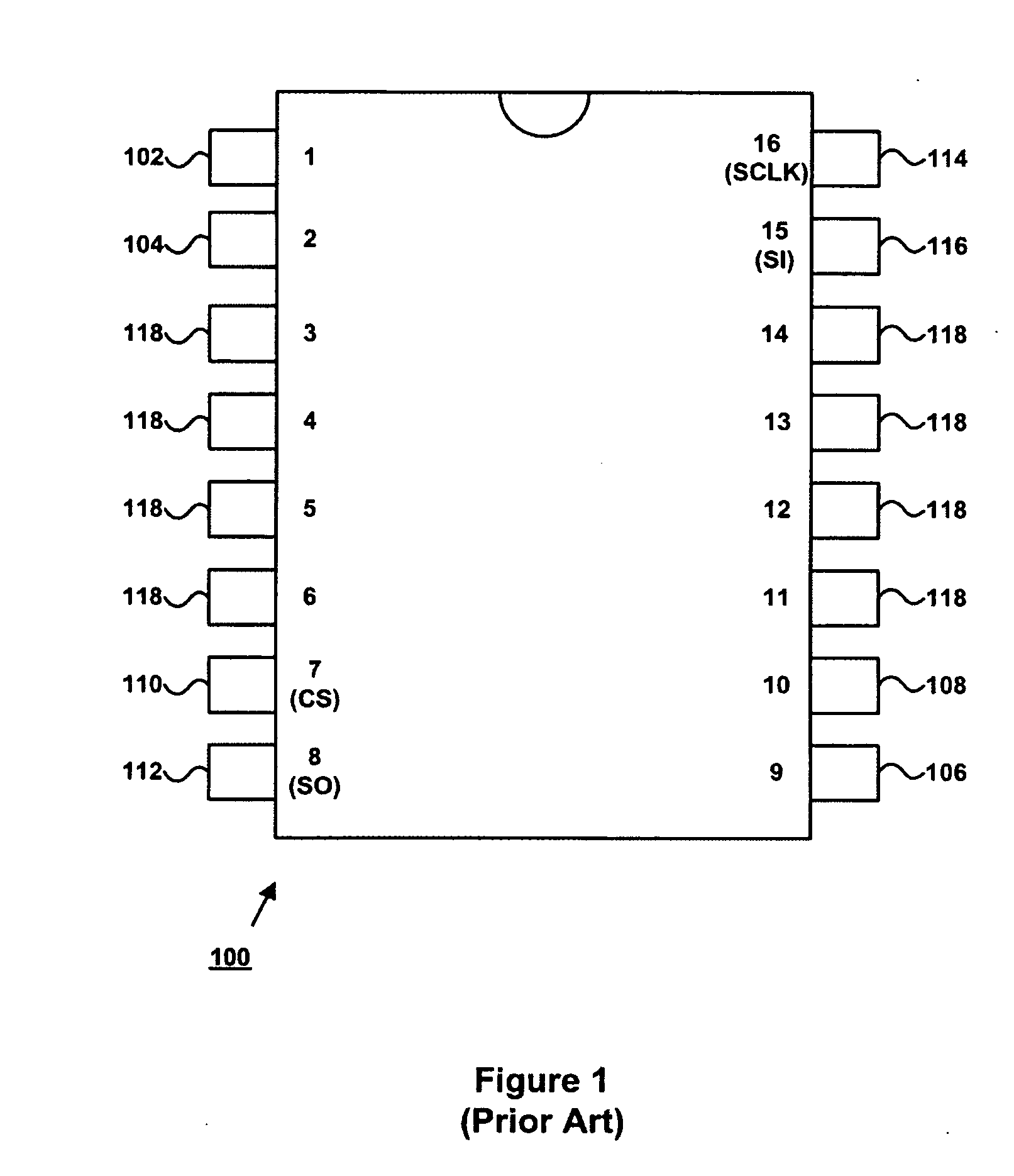
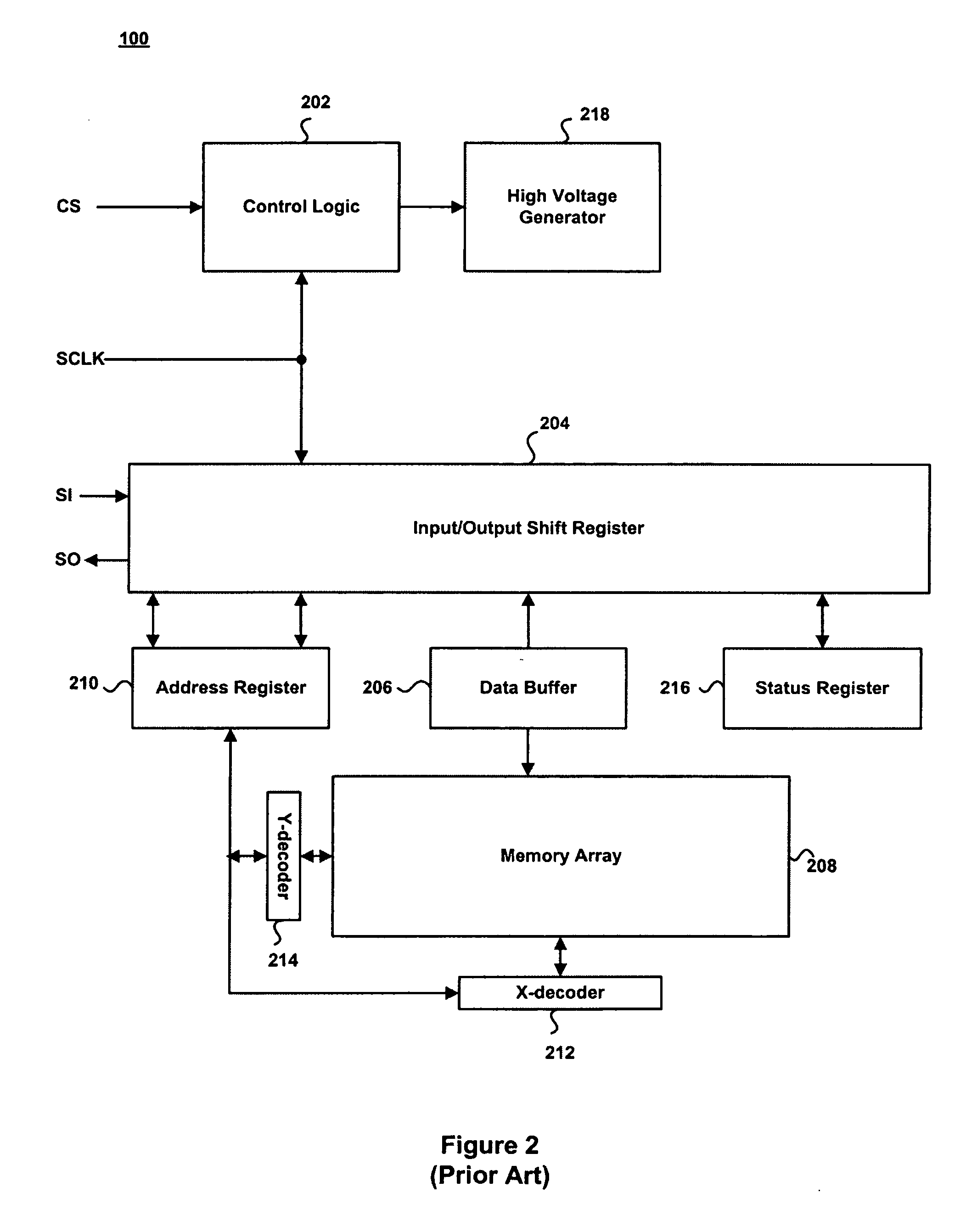
[0004] A serial peripheral interface (SPI) has been utilized in the past for enabling the serial exchange of data between two devices, one referred to as the master and the other referred to as the slave. Serially exchanging data involves transmitting data between the master and slave devices one bit at a time, and is often used in computer systems for transmitting data between the central processing unit (CPU) and various peripheral devices. In such a case, the CPU acts as the master device and the peripherals are the slave devices. The bit-by-bit transmission of data is limited by the speed of the serial clock rate of the master device, so that if the serial clock rate is low, large amounts of data will be transmitted very slowly.

[0005] Another means of transmitting data is through a ...


PUM


Abstract

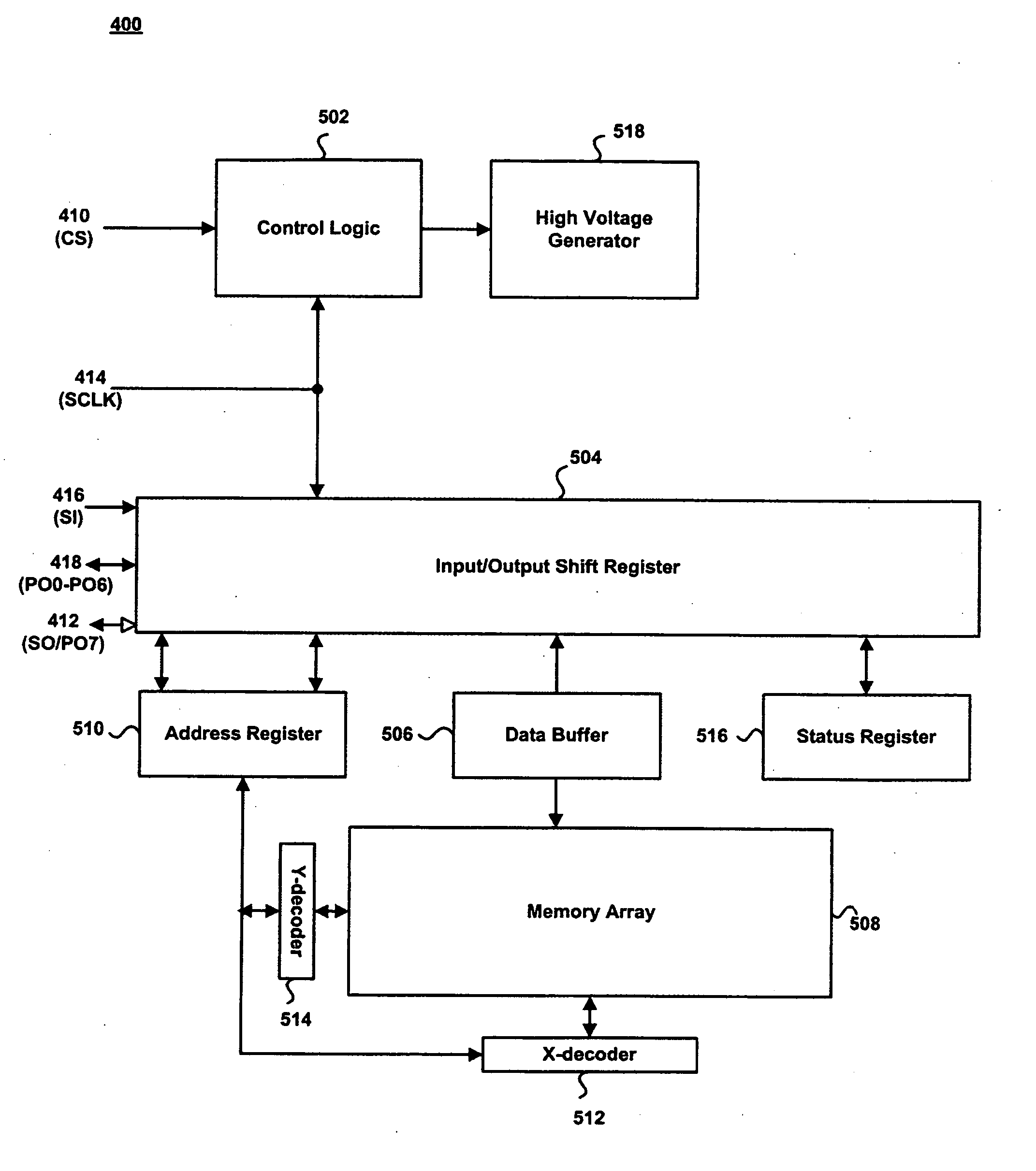
A serial peripheral flash memory device uses a plurality of dummy input / output terminals to enable the selection of a parallel mode for devices that have a slower serial clock speed. In parallel mode, data is transmitted over the plurality of dummy input / output terminals to allow a plurality of bits to be transmitted at the same time improving the data transmission rate at the slower serial clock speed.

Description

DESCRIPTION OF THE INVENTION [0001] 1. Field of the Invention [0002] The invention relates to nonvolatile memory devices that utilize a serial peripheral interface (SPI) for the serial transmission of data. [0003] 2. Background [0004] A serial peripheral interface (SPI) has been utilized in the past for enabling the serial exchange of data between two devices, one referred to as the master and the other referred to as the slave. Serially exchanging data involves transmitting data between the master and slave devices one bit at a time, and is often used in computer systems for transmitting data between the central processing unit (CPU) and various peripheral devices. In such a case, the CPU acts as the master device and the peripherals are the slave devices. The bit-by-bit transmission of data is limited by the speed of the serial clock rate of the master device, so that if the serial clock rate is low, large amounts of data will be transmitted very slowly. [0005] Another means of tr...

Claims


Application Information

Patent Timeline
Patent Type & Authority Applications(United States)
IPC IPC(8): G11C7/00
CPCG11C7/1075G11C5/066
Inventor CHEN, HAN-SUNGYEH, CHIA-YENPO, CHEN-HAOLIN, CHING-CHUNG
Owner MACRONIX INT CO LTD
Learn More