
Photonic sensor particles and fabrication methods

a technology of photonic sensors and fabrication methods, applied in the field of sensing, can solve the problems of many of the components required by such microscopic devices that cannot be fabricated using conventional lithographic tools, and achieve the effect of improving the quality of the finished produ

Inactive Publication Date: 2006-11-16
RGT UNIV OF CALIFORNIA
View PDF10 Cites 38 Cited by
  • Summary
  • Abstract
  • Description
  • Claims
  • Application Information

AI Technical Summary

Benefits of technology

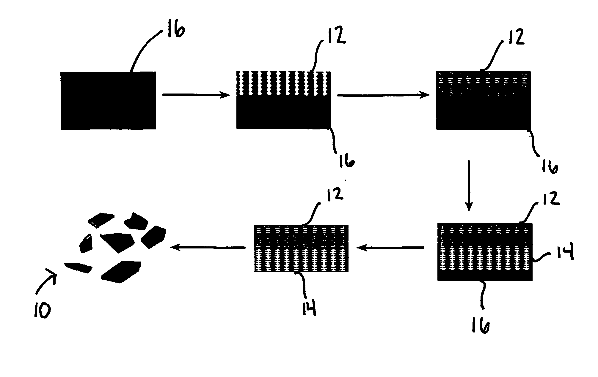
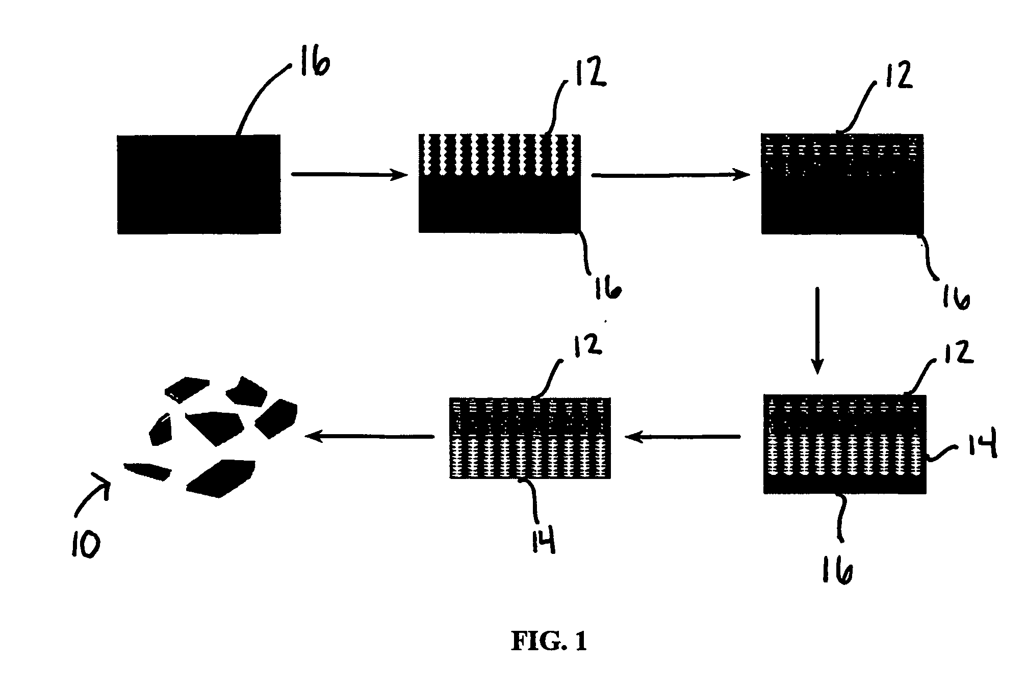
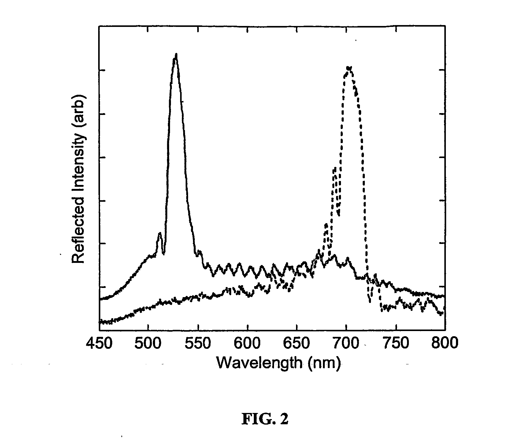
[0004] The invention is related to optical particles, use of optical particles in sensing applications, and methods of fabricating optical particles that can target a desired analyte. The invention is also related to the self-assembly of individual optical particles. An advantage of the invention is that it includes self-assembling individual photonic crystal sensors onto a target. In an embodiment of the invention, a processed sensor structure having two generally opposing surfaces is provided, wherein each of the opposing surfaces have different surface affinities, with a first optical structure formed on one of the opposing surfaces, and a second optical structure formed on the other of the opposing surfaces. The chemically and optically asymmetric opposing surfaces will spontaneously align at an organic liquid / water interface. Changes in the optical response of at least one of the opposing surfaces indicate the presence of a particular analyte for sensing applications.
is that it includes self-assembling individual photonic crystal sensors onto a target. In an embodiment of the invention, a processed sensor structure having two generally opposing surfaces is provided, wherein each of the opposing surfaces have different surface affinities, with a first optical structure formed on one of the opposing surfaces, and a second optical structure formed on the other of the opposing surfaces. The chemically and optically asymmetric opposing surfaces will spontaneously align at an organic liquid / water interface. Changes in the optical response of at least one of the opposing surfaces indicate the presence of a particular analyte for sensing applications.

Problems solved by technology

However, many of the components required by such microscopic devices are too small or overly complex to be fabricated using conventional lithographic tools.

Method used


Image

  • Photonic sensor particles and fabrication methods
  • Photonic sensor particles and fabrication methods
  • Photonic sensor particles and fabrication methods

Examples


Embodiment Construction

[0009] The invention is related to optical particles, use of optical particles in sensing applications, and methods of fabricating optical particles. It is contemplated that the chemically asymmetric optical particles have applications in high throughput screening, drug discovery, biomedical implants, information display, optical switching, and chemical and biological sensor fields. In one embodiment, a processed substrate is provided having two opposing surfaces, such as, for example, a top surface and a bottom surface, with different surface affinities and different optical signatures, with a first optical structure formed on the top surface, and a second optical structure formed on the bottom surface. While the opposing surfaces are discussed as top and bottom surfaces herein for purposes of convention, the invention contemplates use of any two opposite sides, referred to herein as oppositely.

[0010] The top and bottom surfaces are chemically and optically asymmetric. At least on...


PUM

PropertyMeasurementUnit
Timeaaaaaaaaaa
Currentaaaaaaaaaa
Wavelengthaaaaaaaaaa

Abstract

The invention is related to optical particles (10), use of optical particles in sensing applications, and methods of fabricating optical particles that can target a desired analyte. The invention is also related to the self assembly of individual optical particles. An advantage of the invention is that it includes self-assembling individual photonic crystal sensors onto a target. In an embodiment of the invention, a processed sensor structure having two generally opposing surfaces is provided, wherein each of the opposing surfaces have different surface affinities, with a first optical structure formed on one of the opposing surfaces, and a second optical structure formed on the other of the opposing surfaces. The chemically and optically asymmetric opposing surfaces will spontaneously align at an organic liquid / water interface. Changes in the optical response of at least one of the opposing surfaces indicate the presence of a particular analyte for sensing applications.

Description

TECHNICAL FIELD [0001] A field of the invention is sensing. Example applications for particles of the invention include high throughput screening, drug discovery, biomedical implants, information display, optical switching, and chemical and biological sensor fields. BACKGROUND ART [0002] Microscopic devices for moving toward specific, predetermined targets to isolate and detect those targets could be invaluable for a variety of applications, such as environmental monitoring, medical diagnostic, or therapeutic applications. However, many of the components required by such microscopic devices are too small or overly complex to be fabricated using conventional lithographic tools. Manipulation of matter at a nanoscale level is accordingly highly advantageous. [0003] Self-assembly reactions provide one route for constructing 1-, 2-, and 3-dimensional objects in this size regime. For example, covalent bonds between alkanethiols and gold substrates have been used to pattern surfaces in 2 d...

Claims


Application Information

Patent Timeline
IPC IPC(8): C23F1/00G01N30/62A61BB29D11/00G02B6/122
CPCB29D11/00663B82Y20/00G02B6/1225G01N21/774G01N21/4788Y10T428/249969
Inventor LINK, JAMIE R.SAILOR, MICHAEL J.
Owner RGT UNIV OF CALIFORNIA
Learn More