Replaceable probe apparatus for probing semiconductor wafer

Active Publication Date: 2006-03-09
CELADON SYST
View PDF24 Cites 12 Cited by
  • Summary
  • Abstract
  • Description
  • Claims
  • Application Information

AI Technical Summary

Benefits of technology

[0007] In one embodiment, a replaceable probe tile is configured into a self-contained assembly. The assembly includes a chassis body that contains a plurality of probes for probing devices on a wafer, a ceramic dielectric block for supporting the probes, at least one wireguide for guiding a plurality of cables from an external testing equipment into the chassis body, and a plurality of electrical connections for connecting the probes to the cables received in the chassis body. The probe tile is removably mounted in a precise location on a base plate by using a guide mechanism. A user can remove the probe tile and place it into a different location or slot on the base plate to accommodate different die pitches.

Problems solved by technology

As the semiconductor industry grows and devices become more complex, many electrical devices, most commonly semiconductor devices, must be electrically tested, for example, for leakage currents and extremely low operating currents.

Method used


Image

  • Replaceable probe apparatus for probing semiconductor wafer
  • Replaceable probe apparatus for probing semiconductor wafer
  • Replaceable probe apparatus for probing semiconductor wafer

Examples


Embodiment Construction

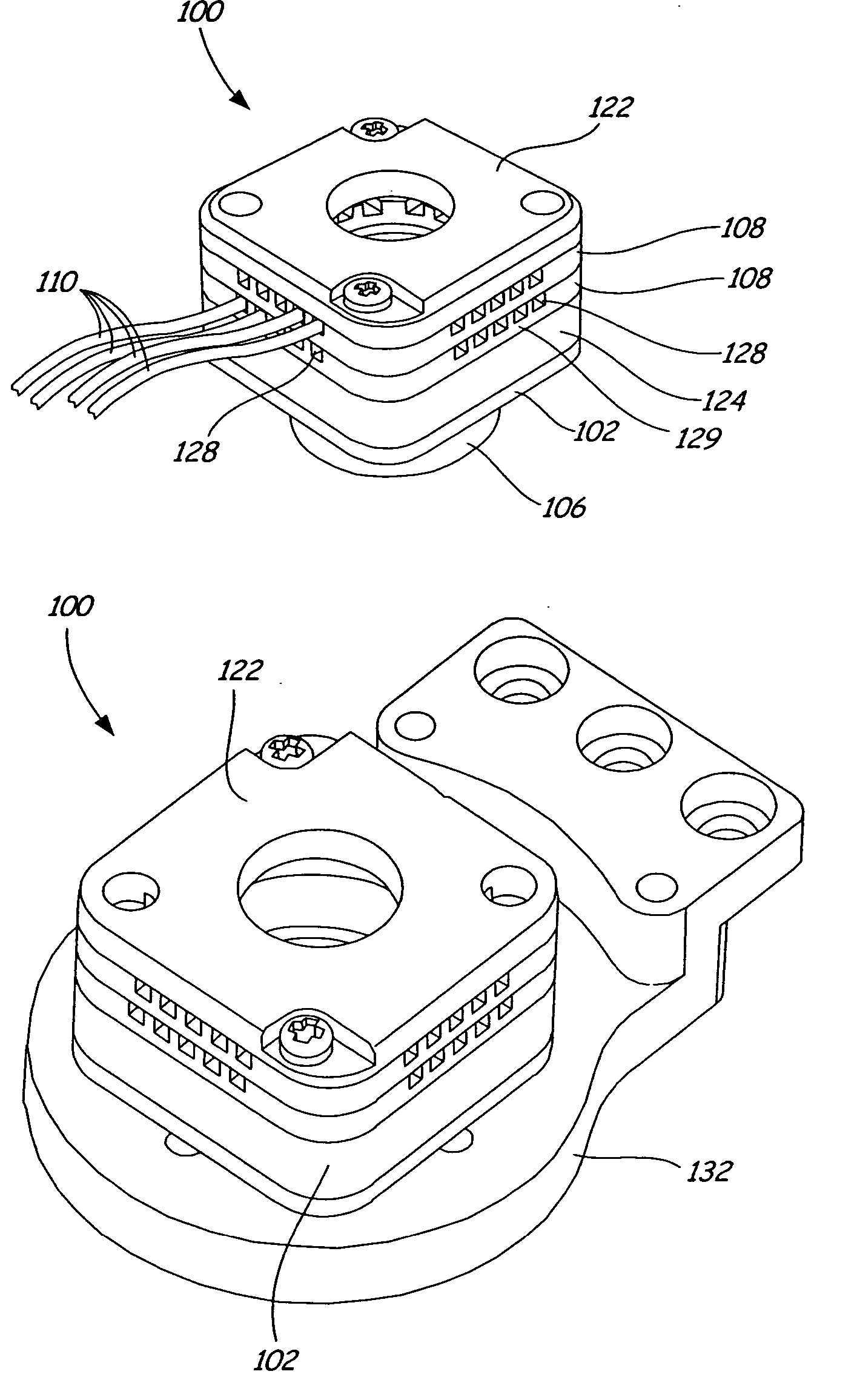
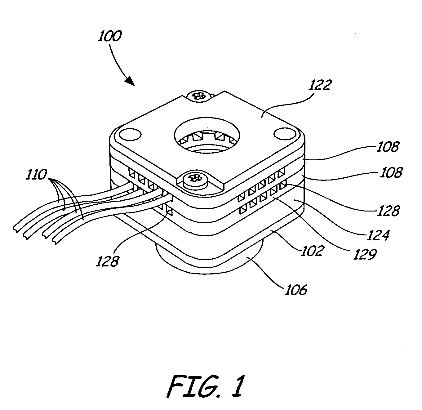
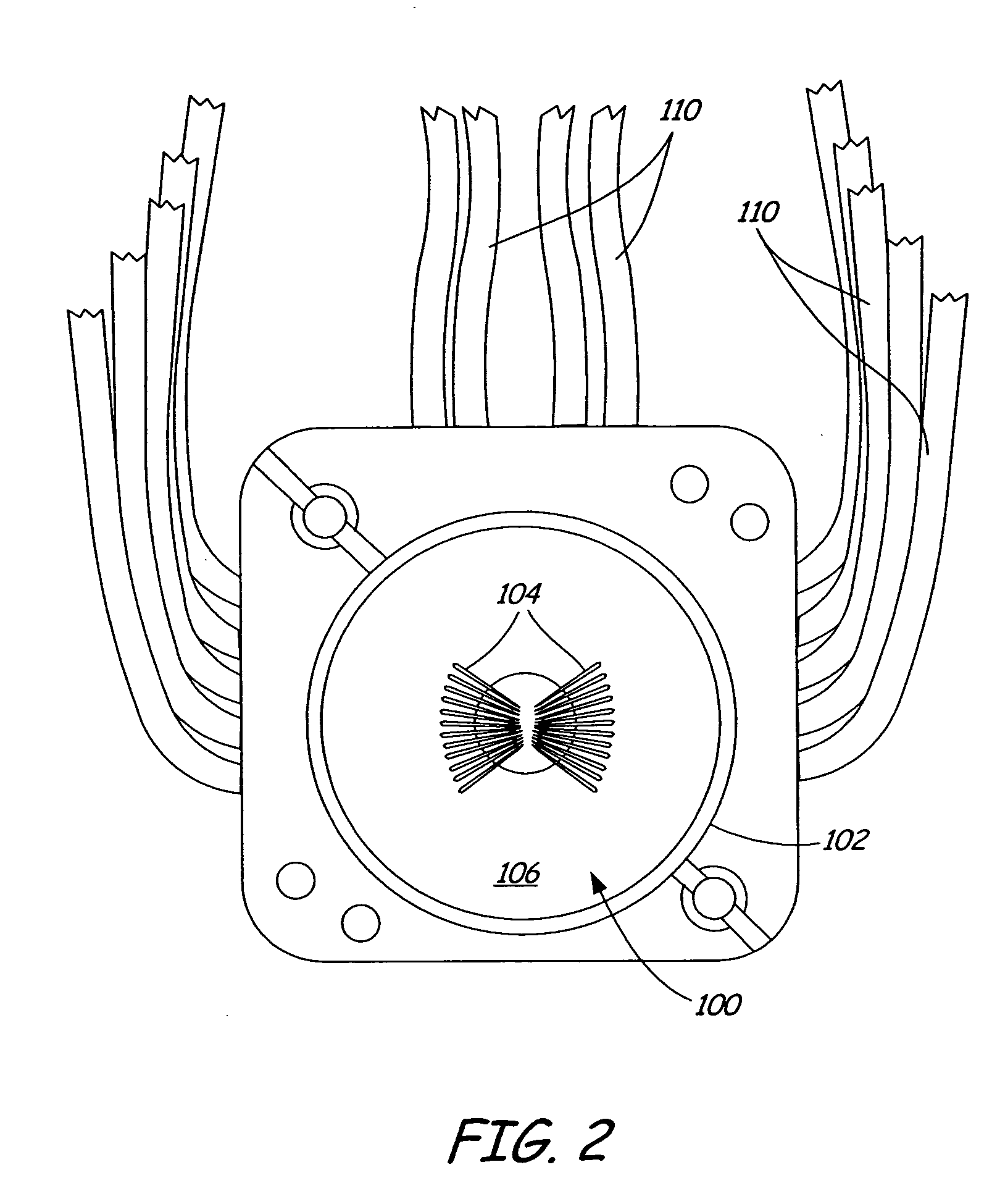
[0031] The present invention provides a probe apparatus having a replaceable probe tile, for testing a device on a semiconductor wafer. FIG. 1 illustrates one embodiment of a replaceable probe tile 100. The probe tile 100 is configured into a self-contained assembly. As shown in FIGS. 1-7, the assembly includes a chassis body 102 that contains a plurality of probes 104 for probing devices on a semiconductor wafer (not shown), a ceramic dielectric block 106 for supporting the probes 104, at least one wireguide 108 for guiding a plurality of cables 110 from an external testing equipment into the chassis body 102, and a plurality of electrical connections (not shown) for connecting the probes 104 to the cables 110 received in the chassis body 102.

[0032] As shown in FIG. 8, the probe tile 100 is removably mounted on a base plate 112. For the purpose of illustration, only the chassis body 102 is shown to be disposed on top of one of locations or slots 114 in the base plate 112. Further,...


PUM


Abstract

A probe apparatus for probing a device on a semiconductor wafer to be tested by a testing equipment is provided. The probe apparatus includes a replaceable probe tile removably mounted in a probing location on a base plate. The probe tile is configured into a self-contained assembly which includes a chassis body containing a plurality of probes for probing devices on a wafer, a dielectric block for supporting the probes, and a wireguide for guiding a plurality of cables from the testing equipment into the chassis body. A wafer station having replaceable base plates and replaceable probe tiles are also provided.

Description

CROSS-REFERENCE TO RELATED APPLICATION(S) [0001] The present patent application claims priority from U.S. Provisional Patent Application, Ser. No. 60 / 606,994, filed Sep. 3, 2004; from U.S. Provisional Patent Application Ser. No. 60 / 607,013, filed Sep. 3, 2004; from U.S. Provisional Patent Application Ser. No. 60 / 607,062, filed Sep. 3, 2004; and is related to U.S. Utility patent application Ser. No. 09 / 730,130, filed on Dec. 4, 2000, now issued U.S. Pat. No. 6,586,954; to U.S. Utility patent application Ser. No. 10 / 601,764, filed on Jun. 23, 2003; to U.S. Utility patent application Ser. No. 09 / 021,631, filed on Feb. 10, 1998, now issued U.S. Pat. No. 6,201,402; to U.S. Utility patent application Ser. No. 10 / 607,768, filed on Jun. 27, 2003; to U.S. patent application Ser. No. 10 / 383,079, filed on Mar. 6, 2003; to U.S. Utility patent application Ser. No. 10 / 809,051, filed on Mar. 25, 2004; subject matter of which are incorporated herewith by references.FIELD OF THE INVENTION [0002] The...

Claims


Application Information

Patent Timeline
Patent Type & Authority Applications(United States)
IPC IPC(8): G01R31/02
CPCG01R1/07364G01R31/2889G01R31/2886
Inventor ROOT, BRYAN J.FUNK, WILLIAM A.
Owner CELADON SYST
Why Eureka
Try Eureka