
Correction method for defects in imagers

a technology of imagers and defects, applied in the field of solid-state imager devices, can solve the problems of reducing the yield of parts during production, causing the creation of defective pixels, and severe image quality degradation

Active Publication Date: 2006-03-02
APTINA IMAGING CORP
View PDF11 Cites 56 Cited by
  • Summary
  • Abstract
  • Description
  • Claims
  • Application Information

AI Technical Summary

Problems solved by technology

During the manufacture of solid state imagers, the creation of defective pixels is unavoidable.
These defective pixels, if not corrected, can cause severe degradation of image quality and, as a result, decrease the yield of parts during production.
However, it is usually less expensive to make a device (e.g., semiconductor imager device) using less precise manufacturing tolerances.
Devices that are produced using less precise manufacturing tolerances, on the other hand, have a higher probability of defects.
Image acquisition semiconductor devices are sensitive to defects and a sensor with defects may not yield aesthetically pleasing images. / It is especially evident when defects are located in low frequency areas or at edges.
A bad pixel in an image acquisition semiconductor device will show up as a bad area on the acquired image.
The defective pixels may not work at all or, alternatively, they may be significantly brighter or dimmer than expected for a given light intensity.
These simple methods, however, are not viable for all pixel defects, such as, for example, those suffering from excessive dark current.
Correction of multiple defective pixels in a small area of an array, termed “cluster defects” or “defective pixel clusters,” however, still remains a significant challenge.

Method used


Image

  • Correction method for defects in imagers
  • Correction method for defects in imagers
  • Correction method for defects in imagers

Examples


Embodiment Construction

[0020] In the following detailed description, reference is made to the accompanying drawings, which form a part hereof and show by way of illustration specific embodiments in which the invention may be practiced. These embodiments are described in sufficient detail to enable those skilled in the art to practice the invention, and it is to be understood that other embodiments may be utilized, and that structural, logical, and electrical changes may be made without departing from the spirit and scope of the present invention. The progression of processing steps described is exemplary of embodiments of the invention; however, the sequence of steps is not limited to that set forth herein and may be changed as is known in the art, with the exception of steps necessarily occurring in a certain order.

[0021] The term “pixel,” as used herein, refers to a photo-element unit cell containing a photosensor device and associated structures for converting photons to an electrical signal. For purp...


PUM


Abstract

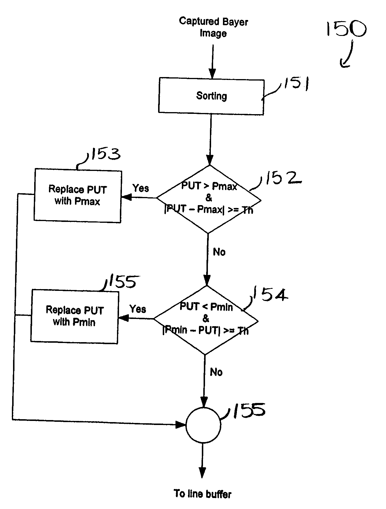
A method and apparatus that allows for the identification and correction of defective pixels and / or pixel clusters in an imaging device. The method, and implementing apparatus determines that a pixel is defective based upon a comparison of its pixel signal value with the value of neighboring pixels. In one exemplary embodiment, a pixel is defective if it is beyond a pre-determined threshold of either a high or low value from its neighboring, corrected pixels. Pixels identified as defective can be corrected using exemplary methods of the invention such as substituting a value of the defective pixel with a value of one of its non-defective neighbors.

Description

FIELD OF THE INVENTION [0001] The invention relates generally to the field of solid state imager devices, and more particularly to methods of identifying and correcting pixel defects in a solid state imager device. BACKGROUND OF THE INVENTION [0002] Solid state imagers, including charge coupled devices (CCD) and CMOS imagers, have been used in photo imaging applications. A solid state imager circuit includes a focal plane array of pixel cells, each one of the cells including a photosensor, which may be a photogate, photoconductor or a photodiode having a doped region for accumulating photo-generated charge. [0003] During the manufacture of solid state imagers, the creation of defective pixels is unavoidable. These defective pixels, if not corrected, can cause severe degradation of image quality and, as a result, decrease the yield of parts during production. Thus, minimization of these defects during fabrication will yield a higher quality product. However, it is usually less expens...

Claims


Application Information

Patent Timeline
IPC IPC(8): H04N9/64
CPCH04N5/367H04N25/68
Inventor YEUNG, CLIFFORDDATAR, SACHIN
Owner APTINA IMAGING CORP
Learn More