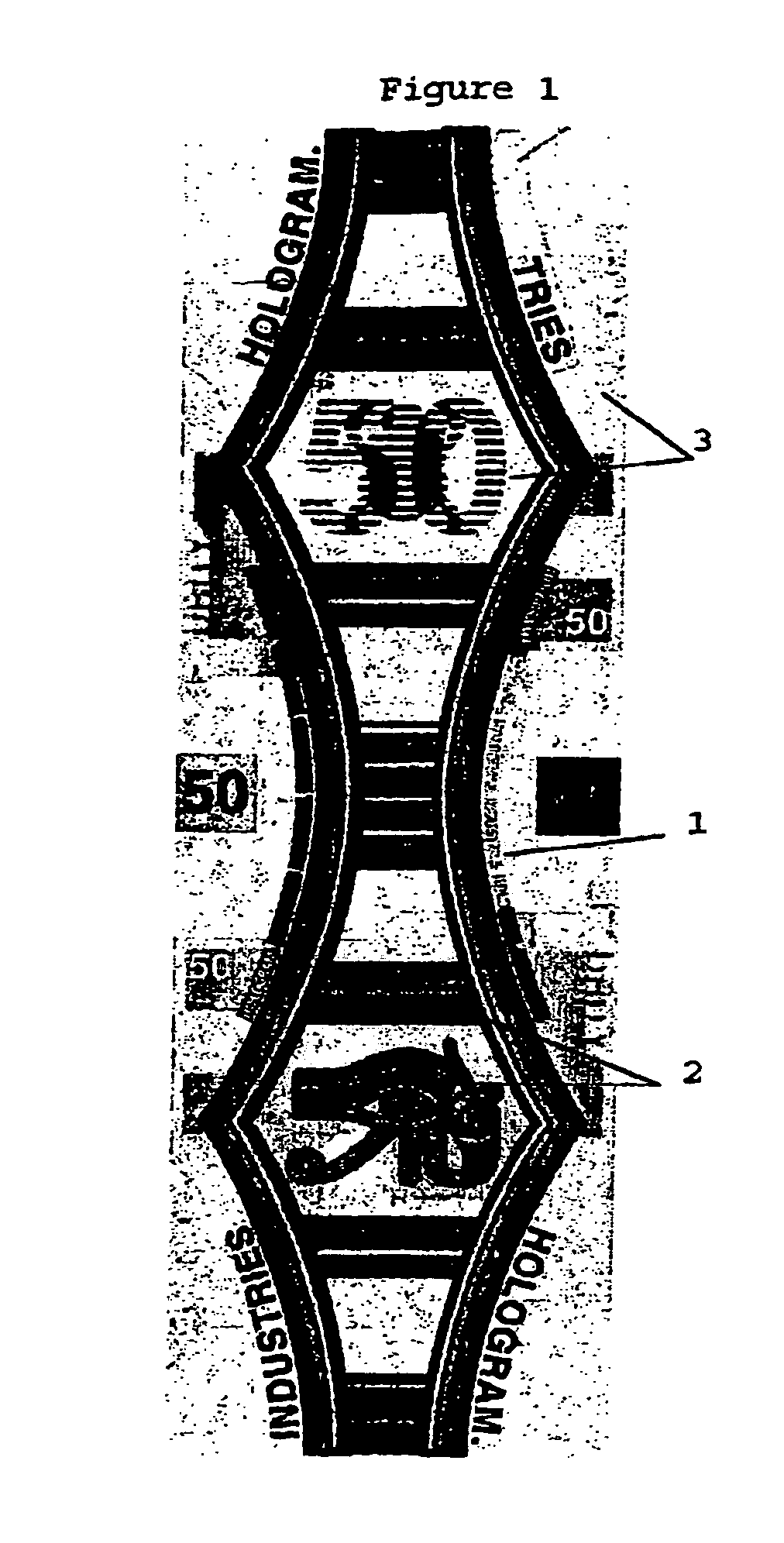
Process producing an optical security component
a technology of optical security and process, applied in the field of document authentication, can solve problems such as difficult reproduction of components, and achieve the effect of high optical index
- Summary
- Abstract
- Description
- Claims
- Application Information
AI Technical Summary
Problems solved by technology
Method used
Image
Examples
Embodiment Construction
[0021] This invention concerns a process for producing an optical security component comprising stamping a transparent film, depositing a layer of dielectric material with a high optical index on the entire surface under a vacuum, partial metallization of the film and an adhering stage, characterized in that the stamping is achieved with a matrix with a first type of zone whose surface state is matte, and a second type of zone whose surface state has cuttings for forming a diffracting network, and in that metallization comprising depositing a layer of metal on only part of the zones of each type whereas the other part remains transparent.
[0022] The stamping is advantageously realized with a matrix with, in addition, a third type of zone whose surface state is smooth.
[0023] According to one aspect, the matrix has, in addition, a fourth type of zone whose surface state is semi-matte with a granularity lower than the matte surface state.
[0024] According to another aspect, some of th...
PUM
| Property | Measurement | Unit |
|---|---|---|
| transparent | aaaaa | aaaaa |
| optical index | aaaaa | aaaaa |
| surface state | aaaaa | aaaaa |
Abstract
Description
Claims
Application Information
 - R&D
- Intellectual Property
- Life Sciences
- Materials
- Tech Scout
- Unparalleled Data Quality
- Higher Quality Content
- 60% Fewer Hallucinations
Browse by: Latest US Patents, China's latest patents, Technical Efficacy Thesaurus, Application Domain, Technology Topic, Popular Technical Reports.
© 2025 PatSnap. All rights reserved.Legal|Privacy policy|Modern Slavery Act Transparency Statement|Sitemap|About US| Contact US: help@patsnap.com

