
RFID tag and method of manufacture

Active Publication Date: 2006-01-05
INTERMEC IP
View PDF15 Cites 64 Cited by
  • Summary
  • Abstract
  • Description
  • Claims
  • Application Information

AI Technical Summary

Benefits of technology

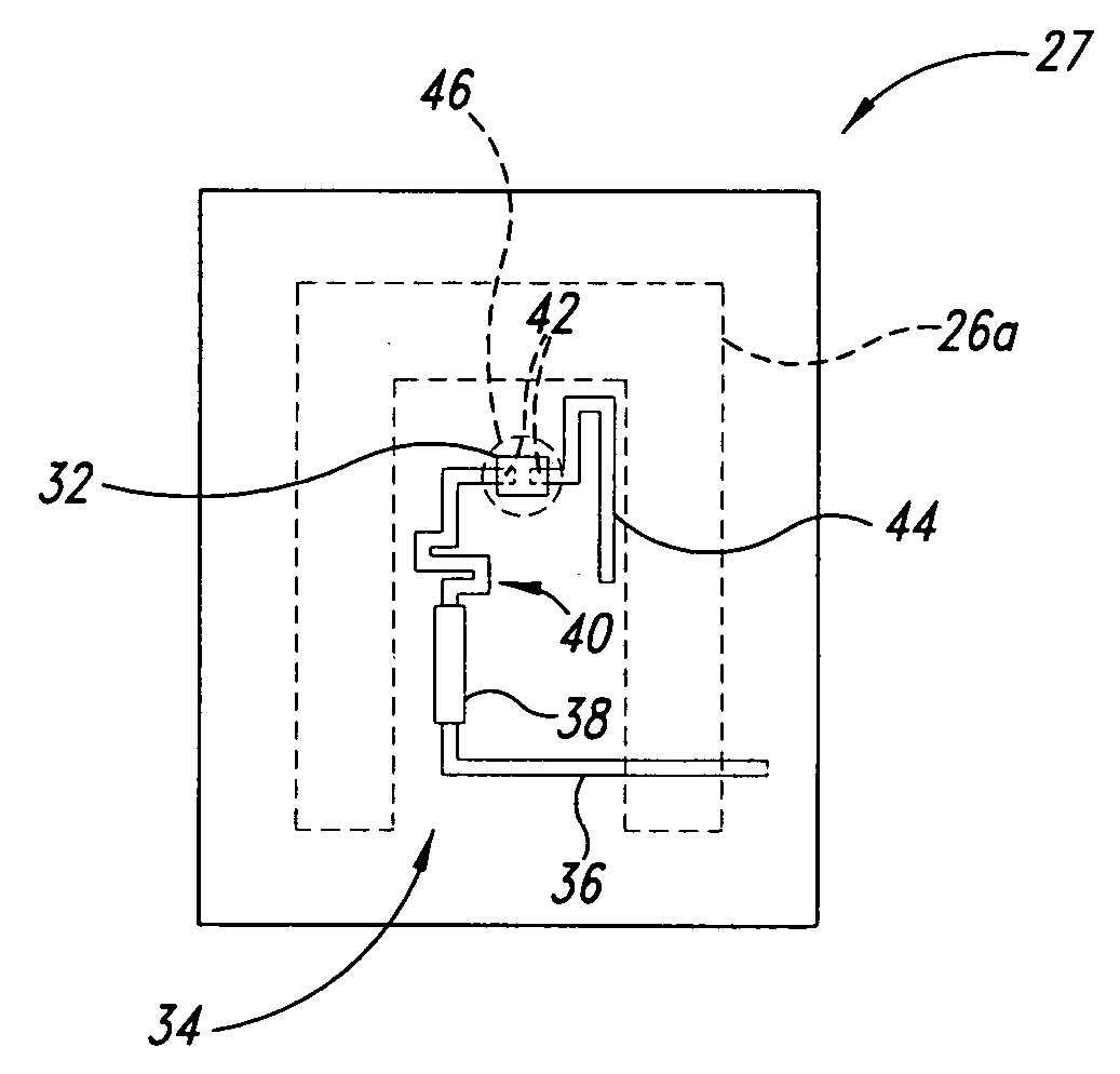
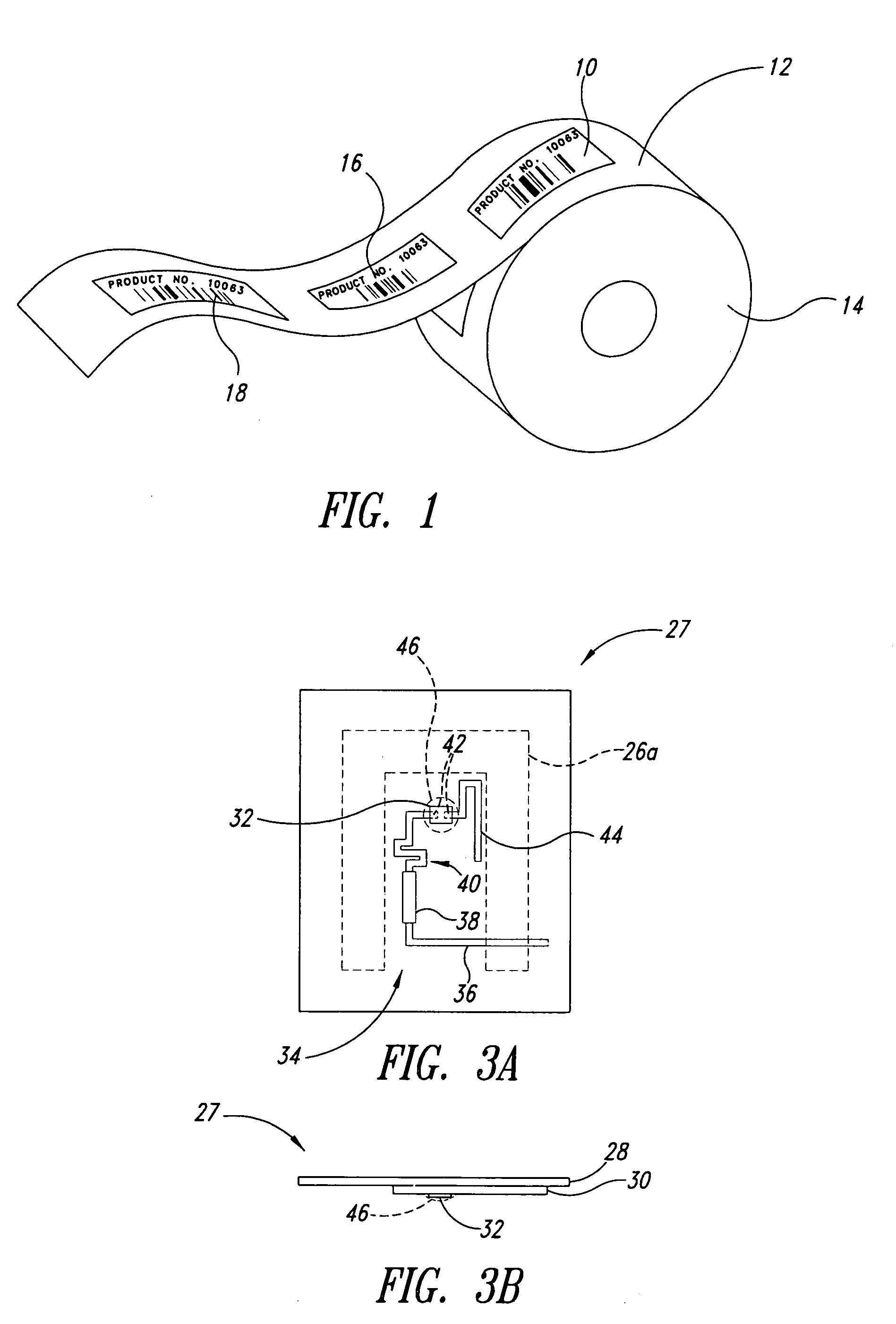
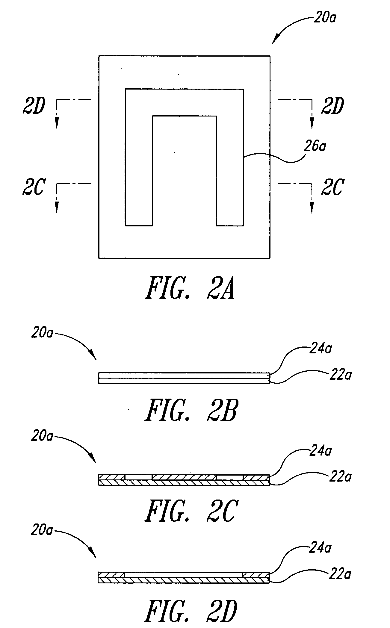
[0007] In one aspect, an RFID tag may be formed from an antenna substrate and a circuit substrate, where the antenna substrate comprises a conductive layer etched to form an antenna, and the circuit substrate comprises a conductive layer etched to form a circuit. The use of separate substrates for the antenna and the circuit may reduce the amount of conductor, and hence the cost, particularly where etching is employed to form the antenna and / or circuit structures. The RFID tag may employ electro-magnetic coupling between the antenna and circuit structures, eliminating the use of vias or through-holes, thereby reducing manufacturing complexity and costs.
[0008] In another aspect, the RFID tag may be formed from an antenna substrate and a circuit substrate, where the antenna substrate comprises a conductive antenna pattern deposited thereon and the circuit substrate comprises a circuit pattern deposited thereon. Again, the use of electromagnetic coupling between the antenna and circuit structures may eliminate the use of vias or through-holes, thereby reducing manufacturing complexity and costs.
[0009] In a further aspect, an RFID tag may be formed from an insert substrate comprising an insulative layer between two conductive layers, a first one of the conductive layers etched to form an antenna and a second one of the conductive layers etched to form a circuit; and a semiconductor device coupled to the circuit. In yet a further aspect, the insert substrate may be received in a label package. A single insulative layer may reduce manufacturing complexity. The use of depositioning rather than etching may reduce the amount of conductive material employed, further reducing costs.

Problems solved by technology

The use of separate substrates for the antenna and the circuit may reduce the amount of conductor, and hence the cost, particularly where etching is employed to form the antenna and / or circuit structures.

Method used


Image

  • RFID tag and method of manufacture
  • RFID tag and method of manufacture
  • RFID tag and method of manufacture

Examples


Embodiment Construction

[0046] In the following description, certain specific details are set forth in order to provide a thorough understanding of various embodiments of the invention. However, one skilled in the art will understand that the invention may be practiced without these details. In other instances, well-known structures associated with RFID tags, antennas, semiconductor devices, memory circuits, and interrogators or readers have not been shown or described in detail to avoid unnecessarily obscuring descriptions of the embodiments of the invention.

[0047] Unless the context requires otherwise, throughout the specification and claims which follow, the word “comprise” and variations thereof, such as, “comprises” and “comprising” are to be construed in an open, inclusive sense, that is as “including, but not limited to.”

[0048] Reference throughout this specification to “one embodiment” or “an embodiment” means that a particular feature, structure or characteristic described in connection with the ...


PUM

PropertyMeasurementUnit
Electrical conductivityaaaaaaaaaa
Electrical conductoraaaaaaaaaa
Adhesivityaaaaaaaaaa

Abstract

An RFID tag may include an antenna substrate comprising a conductive layer etched or deposited to form an antenna, and a circuit substrate comprising a conductive layer etched or deposited to form a circuit, the antenna electro-magnetically coupled to the circuit. An RFID tag may be formed from an insert substrate comprising an insulative layer between two conductive layers, one of the conductive layers etched to form an antenna and the other conductive layer etched to form a circuit. The insert substrate may be received in an envelope formed by a label substrate, which may carry a pressure sensitive adhesive.

Description

BACKGROUND OF THE INVENTION [0001] 1. Field of the Invention [0002] This disclosure generally relates to automatic data collection (ADC) and more particularly to radio frequency identification (RFID). [0003] 2. Description of the Related Art [0004] The ADC arts include a variety of data carrier types for automatically collecting and storing information. One such data carrier takes the form of an RFID tag, which is sometimes provided in the form of a card. Such RFID tags typically include an insert that is received in a label. The insert typically comprises at least one insulative substrate that carries one or more conductive patterns or traces that form an antenna on one side of the insulative substrate, and a semiconductor device including memory carried on the other side of the insulative substrate. The semiconductor device is electrically coupled to the antenna by electrical current paths formed as vias or throughholes in the insulative substrate. The label typically takes the fo...

Claims


Application Information

Patent Timeline
IPC IPC(8): G06K19/06G08B13/14H01R43/00
CPCG06K19/07749Y10T29/49117G06K19/07756
Inventor KODUKULA, VENKATA S. R.LAM, FOR S.MARTINEZ, RENE D.
Owner INTERMEC IP
Learn More