CPP thin-film magnetic head having multilayered conductive layer behind the head and method for producing CPP thin-film magnetic head

Inactive Publication Date: 2005-12-01
TDK CORPARATION
View PDF3 Cites 8 Cited by
  • Summary
  • Abstract
  • Description
  • Claims
  • Application Information

AI Technical Summary

Benefits of technology

[0008] In view of the problem described above, the present invention has been accomplished. It is an object of the present invention to provide a CPP thin-film magnetic head capable of reducing noise of an element output, reducing a resistance that does not contribute to the element output, avoiding damage to the thin-film magnetic head element due to etching, and advantageously reducing an interval between the shield layers, and to provide a method for producing the CPP thin-film magnetic head.
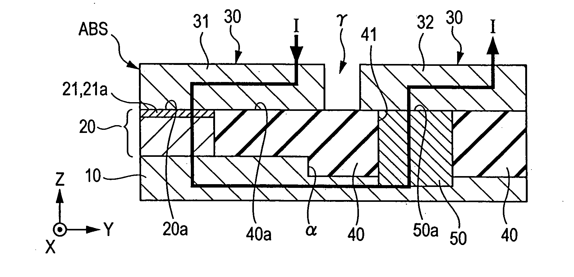
[0011] According to an embodiment, the second top shield sublayer is not in directly contact with the bottom shield layer. The top surface of the metal layer that conductively connects the second top shield sublayer with the bottom shield layer is the contact surface with the second top shield sublayer. Thus, the surface oxide layer on the bottom shield layer and the surface oxide layer on the thin-film magnetic head element can be removed in separate steps. Consequently, it is possible to completely remove the surface oxide layers on the thin-film magnetic head element and the bottom shield layer in the minimum amount of etching without causing damage to the thin-film magnetic head element.
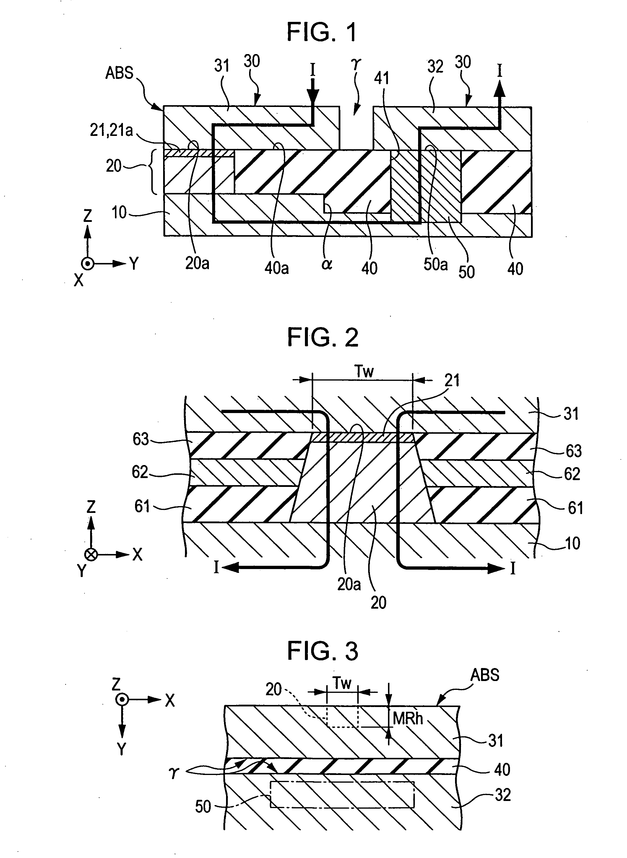
[0013] The size of the metal layer in the track width direction is preferably greater than that of the thin-film magnetic head element in the track width direction. Since this metal layer functions as an electrode together with the bottom shield layer and the second top shield layer, the resistance of the entire electrode can be reduced because of large area thereof.
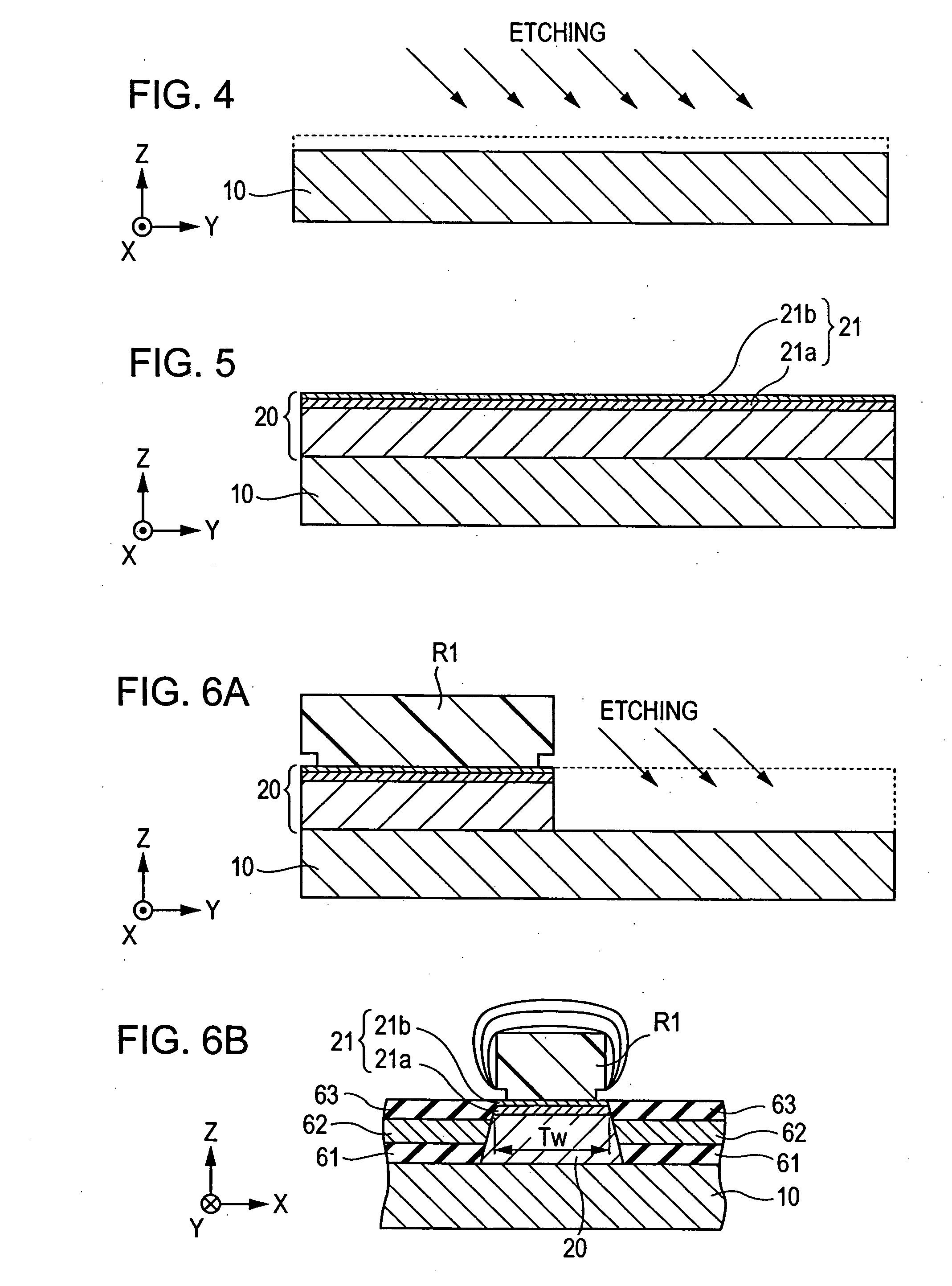
[0017] According to the embodiment described above, the step of removing the surface oxide layer on the bottom shield layer exposed in the space for forming a hole and the step of the surface oxide layer on the thin-film magnetic head element are performed separately, it is possible to surely remove the surface oxide layers on the thin-film magnetic head element and the bottom shield layer without causing damage to the thin-film magnetic head element. Moreover, since the surface oxide layer on the thin-film magnetic head element can be removed in the minimum amount of etching, there in no need to provide a thick cap layer, which is the uppermost layer of the thin-film magnetic head element. This is advantageous in reducing the interval between the shield layers. Since no oxide layer is present in the current path through the thin-film magnetic head element, a resistance that does not contribute to the element output and the output noise of the element due to a change in the resistance are reduced.
[0019] The uppermost layer of the thin-film magnetic head element is preferably formed of a cap layer having a laminate structure containing a ruthenium film and a tantalum film. Then, in the step of removing the surface oxide layer on the metal layer, the tantalum film of the cap layer being completely removed to expose the ruthenium film, and then the first top shield sublayer being formed on the ruthenium film. To suppress the amount of etching for removing the surface oxide layer, the cap layer is preferably composed of a material, for example, ruthenium, having oxidation resistance. However, when ruthenium material is exposed at the top surface of the cap layer, photolithography is insufficiently performed. Thus, a tantalum film capable of being suitably processed by photolithography is stacked on the ruthenium film. Then, immediately before forming the first top shield sublayer, the tantalum film is completely removed.
[0020] The present invention provides a CPP thin-film magnetic head capable of reducing output noise of the element, reducing a resistance that does not contribute to the element output, avoiding damage to the thin-film magnetic head element due to etching, and advantageously reducing an interval between the shield layers, and provides a method for producing the CPP thin-film magnetic head.

Problems solved by technology

However, an increase in the amount of etching for the complete removal of the surface oxide layer on the bottom shield layer 110 results in the deeply etched surface of the thin-film magnetic head element 120, thus causing great damage to the element.
In view of magnetic shielding effect and the like, it is difficult to use the above-described material having oxidation resistance as the shield material in the present circumstances.

Method used


Image

  • CPP thin-film magnetic head having multilayered conductive layer behind the head and method for producing CPP thin-film magnetic head
  • CPP thin-film magnetic head having multilayered conductive layer behind the head and method for producing CPP thin-film magnetic head
  • CPP thin-film magnetic head having multilayered conductive layer behind the head and method for producing CPP thin-film magnetic head

Examples


Embodiment Construction

[0033] The present invention will be described based on the drawings. In the respective drawings, the x-direction is a track width direction. The y-direction is the height direction (direction of leakage flux from a storage medium). The z-direction is the direction to which the storage medium moves and the stacking direction of layers constituting the thin-film magnetic head.

[0034] FIGS. 1 to 3 each show a CPP thin-film magnetic head according to an embodiment of the present invention. FIG. 1 is a fragmentary sectional view through the center of a CPP thin-film magnetic head according to an embodiment of the present invention. FIG. 2 is a fragmentary sectional view of the CPP thin-film magnetic head shown in FIG. 1 when viewed from the surface of the head opposite a storage medium. FIG. 3 is a schematic plan view of the CPP thin-film magnetic head when viewed from above.

[0035] The CPP thin-film magnetic head includes a bottom shield layer 10 and a top shield layer 30 disposed at a...


PUM

PropertyMeasurementUnit
Thicknessaaaaaaaaaa
Sizeaaaaaaaaaa
Electrical conductoraaaaaaaaaa

Abstract

A CPP thin-film magnetic head includes a bottom shield layer; a top shield layer, the bottom shield layer and the top shield layer being disposed at a predetermined interval; a thin-film magnetic head element between the bottom shield layer and the top shield layer; an insulating layer behind the thin-film magnetic head element in the height direction and disposed between the bottom shield layer and the top shield layer; and a metal layer in the insulating layer, the top shield layer including a first top shield sublayer on the thin-film magnetic head element; and a second top shield sublayer behind the first top shield sublayer in the height direction, the second top shield sublayer and the bottom shield layer being conductively connected through the metal layer, wherein a current flows in the direction orthogonal to a surface of a layer constituting the thin-film magnetic head element.

Description

BACKGROUND OF THE INVENTION [0001] 1. Field of the Invention [0002] The present invention relates to a CPP thin-film magnetic head in which a sense current flows in the thickness direction (direction orthogonal to the film surface) and a method for producing the CPP thin-film magnetic head. [0003] 2. Description of the Related Art [0004] Giant magnetoresistive devices (GMR devices) and tunneling magnetoresistive devices (TMR devices), which are used as thin-film magnetic heads, can be broadly divided into a current-in-plane (CIP) mode device, in which a sense current flows in the direction parallel to a surface of a layer constituting the device; and a current-perpendicular-to-plane mode deviate, in which a sense current flows in the direction perpendicular to a surface of a layer constituting the device. [0005]FIG. 11 is a fragmentary sectional view of a traditional CPP thin-film magnetic head. The CPP thin-film magnetic head includes a bottom shield layer 110, a top shield layer 1...

Claims


Application Information

Patent Timeline
IPC IPC(8): G11B5/127G11B5/33G11B5/39
CPCG11B5/3903Y10T29/49052Y10T29/49048Y10T29/49043Y10T29/49046
Inventor NISHIYAMA, YOSHIHIRO
Owner TDK CORPARATION
Why Eureka
Try Eureka