Nonvolatile semiconductor memory device including ferroelectric semiconductor pattern and methods for writing data in and reading data from the same

a technology of ferroelectric semiconductor and memory device, which is applied in the field of nonvolatile semiconductor memory device, can solve the problems of difficult development of next-generation memory device, difficult to develop volatile memory device, and laborious research for commonly used memory devi

Inactive Publication Date: 2005-11-17
DONGGUK UNIVERSITY
View PDF8 Cites 6 Cited by
  • Summary
  • Abstract
  • Description
  • Claims
  • Application Information

AI Technical Summary

Benefits of technology

[0010] In the present invention, the nonvolatile semiconductor memory device is formed using a ferroelectric semiconductor material, which has both ferroelectricity and semiconductivity. The ferroelectric semiconductor material, which has a dielectric polarization, forms a hysteresis loop according to an electric field applied thereto. Thus, even if the applied electric field is removed, a double stable polarization state is maintained. Also, since the ferroelectric semiconductor material has semiconductivity, it functions as a resistor by free carriers included in crystalline lattices thereof. The ferroelectric semiconductor material as the resistor forms a Schottky contact or an ohmic contact at an interface with a metal layer. In particular, when the Schottky contact is formed at the interface between the ferroelectric semiconductor material and the metal layer, a contact resistance varies with a polarization state of the ferroelectric semiconductor material and a direction in which an electric field is applied thereto. The present invention utilizes a double characteristic of the ferroelectric semiconductor material.

Problems solved by technology

However, the volatile memory devices are reaching a technical limit due to volatility of data.
And, since the ERPOMs, EEPROMs, and flash EEPROMs, which are lowly integrated, operate at low speed, and / or require a high voltage, it is difficult to develop them into next generation memory devices.
To overcome the limit, laborious research for the commonly used memory devices has progressed in many colleges and laboratories.

Method used


Image

  • Nonvolatile semiconductor memory device including ferroelectric semiconductor pattern and methods for writing data in and reading data from the same
  • Nonvolatile semiconductor memory device including ferroelectric semiconductor pattern and methods for writing data in and reading data from the same
  • Nonvolatile semiconductor memory device including ferroelectric semiconductor pattern and methods for writing data in and reading data from the same

Examples


Embodiment Construction

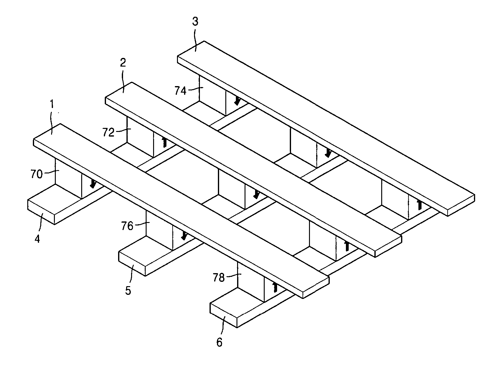
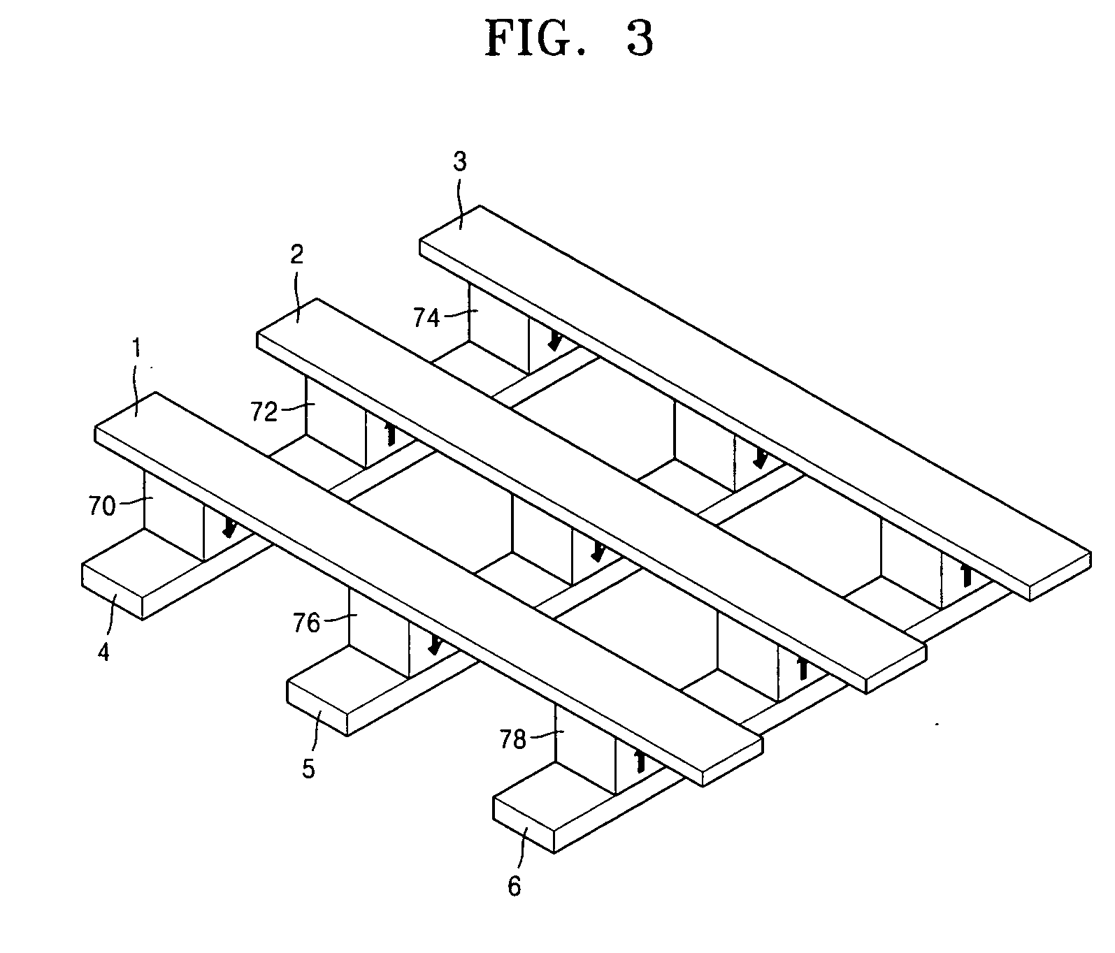
[0018] The present invention will now be described more fully with reference to the accompanying drawings, in which exemplary embodiments of the invention are shown. This invention may, however, be embodied in many different forms and should not be construed as being limited to the embodiments set forth herein. Rather, these embodiments are provided so that this disclosure is thorough and complete and fully conveys the concept of the invention to those skilled in the art. In the drawings, the thicknesses of layers may be exaggerated for clarity, and the same reference numerals are used to denote the same elements throughout the drawings.

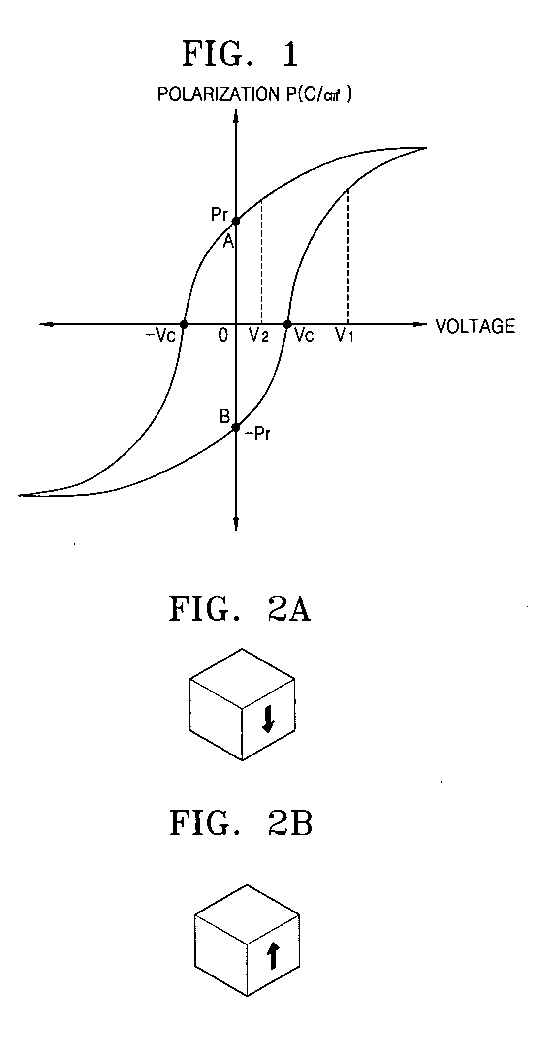
[0019]FIG. 1 is a hysteresis loop curve showing polarization versus voltage of a ferroelectric semiconductor material contained in a memory cell of a nonvolatile semiconductor memory device according to an embodiment of the present invention. For example, the ferroelectric semiconductor material may be CdZnTe.

[0020] Referring to FIG. 1, it can be s...


PUM


Abstract

Provided are a nonvolatile semiconductor memory device including ferroelectric semiconductor patterns in respective memory cells and methods of writing and reading data. The device includes a substrate; a plurality of first conductive lines disposed in or on the substrate; a plurality of second conductive lines disposed in or on the substrate and having a different height from the first conductive lines, wherein the second conductive lines intersect the first conductive lines, respectively, to define a plurality of intersection regions; and a plurality of memory cells disposed on the substrate. Herein, the memory cells include ferroelectric semiconductor patterns, respectively, which are disposed between the first conductive lines and the second conductive lines that define the intersection regions.

Description

[0001] This application claims the priority of Korean Patent Application No. 10-2004-0033799, filed on May 13, 2004, in the Korean Intellectual Property Office, the disclosure of which is incorporated herein in its entirety by reference. BACKGROUND OF THE INVENTION [0002] 1. Field of the Invention [0003] The present invention relates to a semiconductor memory device, and more particularly, to a nonvolatile semiconductor memory including ferroelectric semiconductor patterns in respective memory cells and methods of writing data in the memory cells and reading data from the memory cells. [0004] 2. Description of the Related Art [0005] Semiconductor memory devices can be categorized into volatile memory devices and nonvolatile memory devices. Unlike the volatile memory devices, the nonvolatile memory devices can retain data even if power is not supplied. Some volatile memory devices, such as DRAMs or SRAMs, and some nonvolatile memory devices, such as EPROMs, EEPROMs, and flash EEPROMs...

Claims


Application Information

Patent Timeline
Patent Type & Authority Applications(United States)
IPC IPC(8): H01L27/105G11C5/00G11C11/22
CPCG11C11/22A47G19/027A47G19/04A47G2400/04A47G2400/064
Inventor LEE, JAE CHOONFU, DE JUNKANG, TAE WONLEE, SEUNG JOOHEO, YOO BUMKIM, DAE HOONLEE, JU WONLEE, DONG JIN
Owner DONGGUK UNIVERSITY
Why Eureka
Try Eureka