
Optical offset signal cancellation for optical receiver

a technology of optical receiver and offset cancellation, applied in the field of optical interconnects, can solve the problems of insufficient consideration of prior art optical communication systems, the performance bottleneck of electrical interconnects, and the inability to provide the advantage of duplication of existing electrical interconnects

Inactive Publication Date: 2005-10-20
INTEL CORP
View PDF5 Cites 8 Cited by
  • Summary
  • Abstract
  • Description
  • Claims
  • Application Information

AI Technical Summary

Problems solved by technology

As semiconductor technology and advanced computing architectures have resulted in processors that operate at frequencies in multiples of GHz, electrical interconnects have become performance bottlenecks.
If the optical components are not available in cost competitive technologies that are compatible with other components of the information system, they provide little advantage over duplication of existing electrical interconnects.
Such considerations have not been sufficiently addressed in prior art optical communication systems.

Method used


Image

  • Optical offset signal cancellation for optical receiver
  • Optical offset signal cancellation for optical receiver
  • Optical offset signal cancellation for optical receiver

Examples


Embodiment Construction

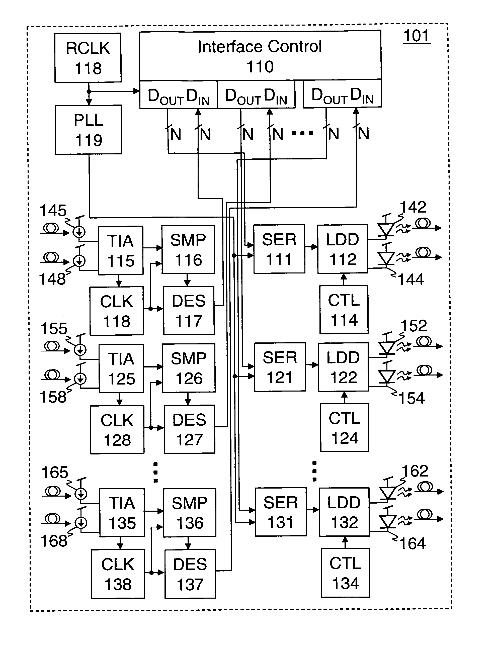
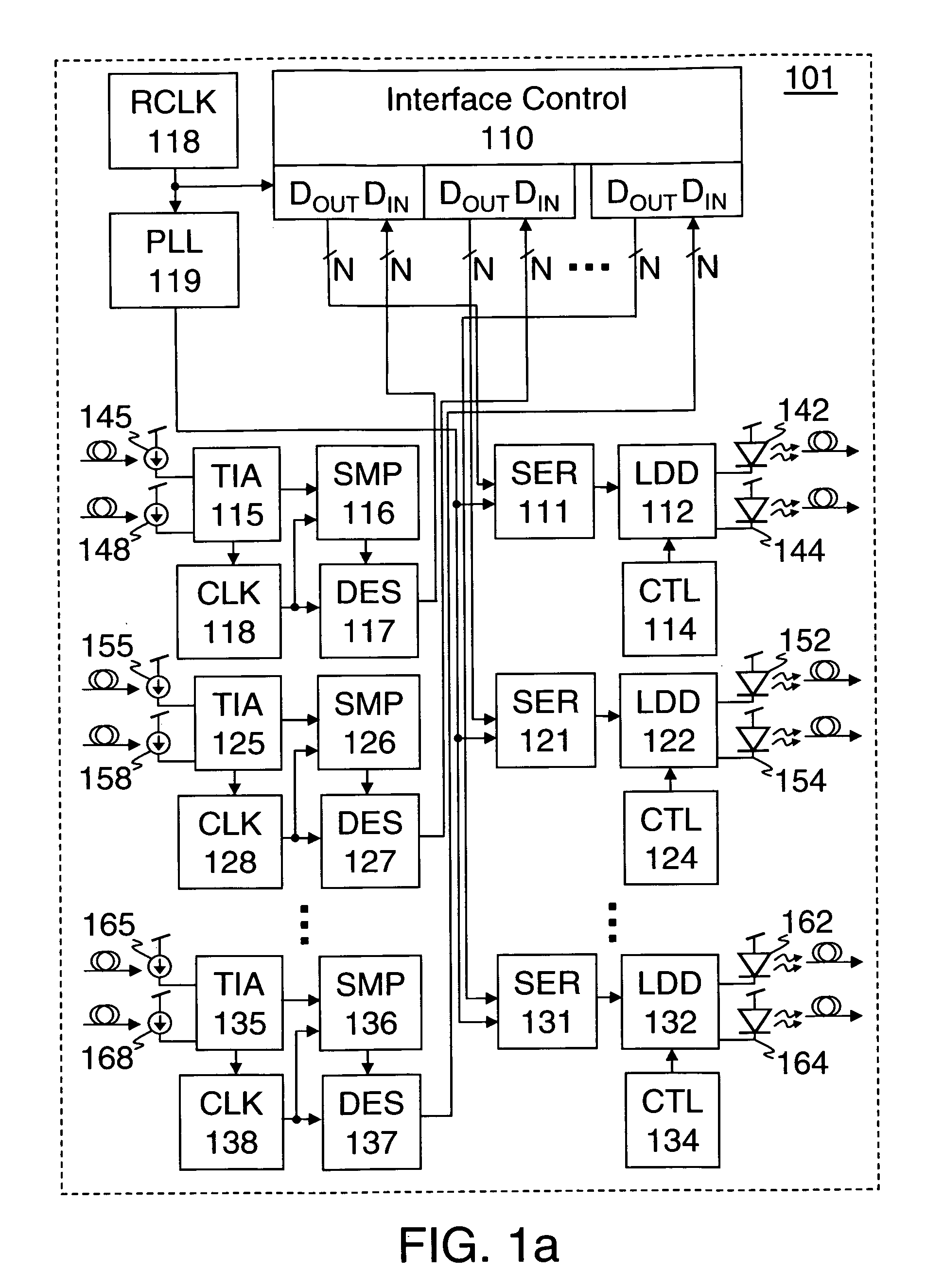
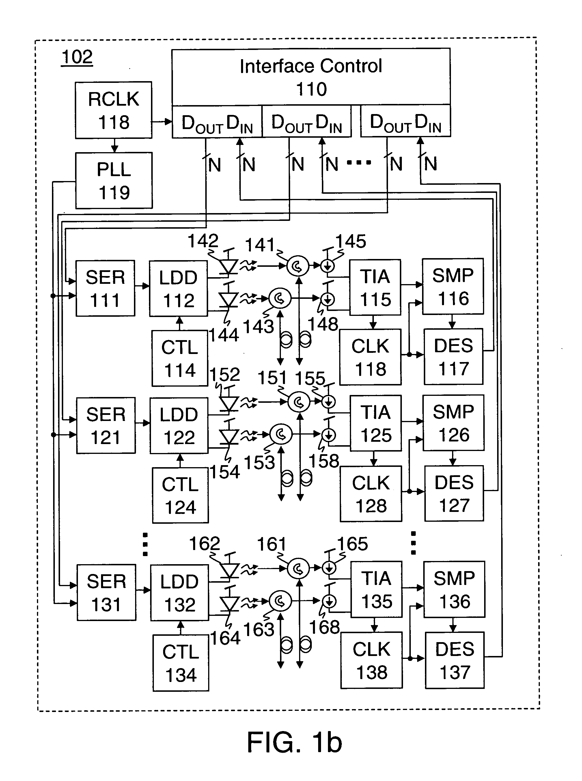
[0029] Methods and apparatus for optical signaling are disclosed herein. In one embodiment comprising a transmitter, a laser driver converts a digital voltage sequence to a current signal having a bias mode adjustable by a bias control and a modulation mode adjustable by a modulation control. A laser generates an optical signal responsive to the current signal of the laser driver. One embodiment of a laser driver for high speed optical interconnections includes a buffered level shifter (BLS) to shift the input voltage level to an appropriate level. In some embodiments the BLS may be tuned to provide a desired level shift with an impedance matched to the driving load. In some embodiments circuitry may also be provided to reduce any overshoot of the output signal and / or to reduce a frequency dependent part of the impedance seen by the AC signals

[0030] In one alternative embodiment comprising a receiver, a photo-detector receives an optical signal and generates a single ended current ...


PUM


Abstract

A laser driver for high speed interconnections may convert a digital signal to a current train of a bias mode to represent logical zero and of a modulation mode to represent logical one. An optical signal thus produced may include an optical offset. An optical receiver may include a photo-detector to receive the optical signal and generate a current signal, which includes a corresponding current offset. A first amplifier stage converts the current signal to a voltage signal and a second amplifier stage generates a digital output from the voltage signal. One or more low-pass filters may be used to filter the digital output and generate a filtered offset signal for a differential amplifier to generate an offset cancellation signal. The offset cancellation signal may be provided to offset cancellation circuitry to remove the current offset from the current signal generated by the photo-detector.

Description

RELATED APPLICATIONS [0001] This is a continuation-in-part claiming, under 35 U.S.C. § 120, the benefit of the filing date of application Ser. No. 10 / 816,026 and of application Ser. No. 10 / 816,321, which were filed on Mar. 31, 2004 and are currently pending.FIELD OF THE DISCLOSURE [0002] This disclosure relates generally to the field of optical interconnects. In particular, the disclosure relates to an optical receiver with a current offset cancellation. BACKGROUND OF THE DISCLOSURE [0003] In the past decade optical communications has become an integral technology component for information systems. As semiconductor technology and advanced computing architectures have resulted in processors that operate at frequencies in multiples of GHz, electrical interconnects have become performance bottlenecks. [0004] In 1998, researchers at Bell Labs transmitted 100 simultaneous optical signals using dense wave-division multiplexing over a distance of 400 km, each signal transmitted at a rate o...

Claims


Application Information

Patent Timeline
IPC IPC(8): H04B10/00H04B10/158
CPCH04B10/66
Inventor PAILLET, FABRICEKARNIK, TANAYXU, JIANPINGGARDNER, DONALD S.
Owner INTEL CORP
Learn More