Thin film device, integrated circuit, electrooptic device, and electronic device

a thin film device and integrated circuit technology, applied in the direction of optics, transistors, instruments, etc., can solve the problems of short distance between the thin film elements included in each adjoining layer, hinder the stable operation of the thin film device, and the above-ground thin film device has problems, so as to avoid the influence of heat generated. , to achieve the effect of stable operation

Inactive Publication Date: 2005-10-20
SEIKO EPSON CORP
View PDF6 Cites 32 Cited by
  • Summary
  • Abstract
  • Description
  • Claims
  • Application Information

AI Technical Summary

Benefits of technology

[0005] Aspects of the present invention provide a thin film device that can secure stable operation by avoidin

Problems solved by technology

However, the above thin film device has problems.
That is, the distance between thin film elements included in each of adjoining layers becomes very short.
Therefore, the influen

Method used


Image

  • Thin film device, integrated circuit, electrooptic device, and electronic device
  • Thin film device, integrated circuit, electrooptic device, and electronic device
  • Thin film device, integrated circuit, electrooptic device, and electronic device

Examples


Embodiment Construction

[0026] Hereinafter, an illustrative embodiment for putting the present invention into practice is described with reference to the accompanying drawings. It is noted that various connections are set forth between elements in the following description. It is noted that these connections in general and, unless specified otherwise, may be direct or indirect and that this specification is not intended to be limiting in this respect.

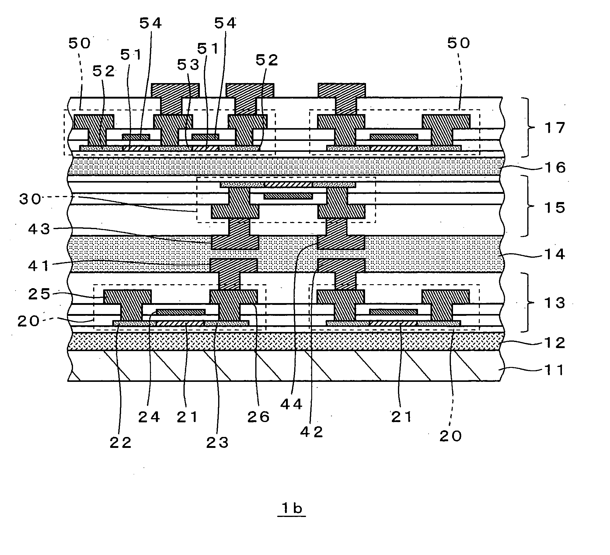
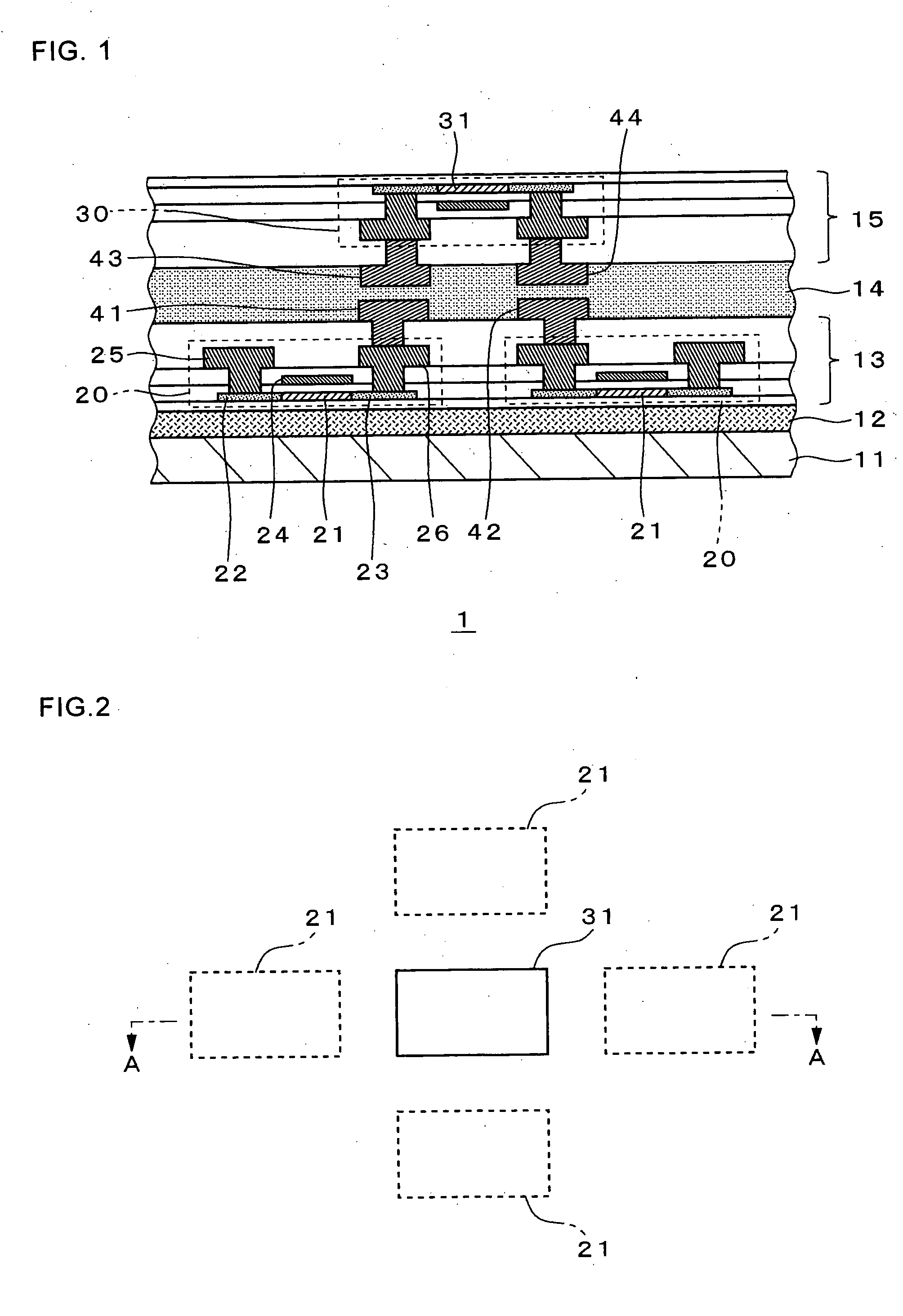
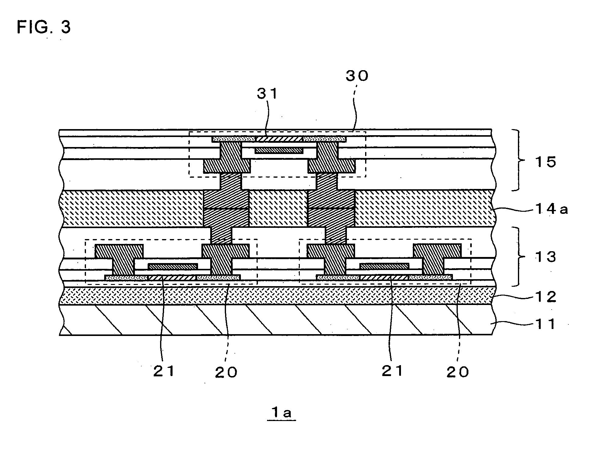
[0027]FIG. 1 is a cross-sectional view showing a configuration of a thin film device according to an illustrative embodiment of the invention. A thin film device 1 shown in FIG. 1 is configured by laminating thin film element layers 13 and 15, each of which includes one or a plurality of thin film transistors, onto an insulation substrate 11, which can be a glass substrate or an epoxy substrate. In addition, FIG. 1 shows laminating multiple thin film layers. This technique can be used to laminate three or more thin film element layers. The thin film element l...


PUM


Abstract

A thin film device including a plurality of thin film element layers having one or more thin film elements, wherein each of the thin film elements has one or more heat generating regions that generates heat when supplied with an electric current is provided. Each of the thin film elements is relatively placed so that the heat generating regions of the thin film elements included in one of two adjoining two thin film element layers does not overlap with the heat generating regions of the thin film elements included in the other thin film element layer in a direction of thickness of the thin film element layers.

Description

RELATED APPLICATIONS [0001] This application claims priority to Japanese Application Nos. 2004-122052, filed Apr. 16, 2004 and 2005-20988, filed Jan. 28, 2005, whose contents are explicitly incorporated herein by reference. FIELD OF THE INVENTION [0002] The present invention relates to a three-dimensional thin film device constructed by laminating circuit layers including thin film transistors and other thin film circuit elements. BACKGROUND OF THE INVENTION [0003] The development of a three-dimensional thin film device that is constructed by laminating thin film element layers including thin film transistors and other thin film elements has been in progress. For example, a method for manufacturing a three-dimensional device by forming a transferring layer, which includes a thin film element, on a substrate, which is to become the source of transfer, and then transferring the transferring layer onto another substrate, which is to become the destination of transfer, is disclosed in J...

Claims


Application Information

Patent Timeline
IPC IPC(8): H01L21/02H01L21/20H01L21/336G02F1/1368H01L21/58H01L21/60H01L21/68H01L21/77H01L21/822H01L21/8234H01L21/84H01L27/00H01L27/04H01L27/08H01L27/088H01L27/12H01L29/04H01L29/786H01L31/036H01L31/20
CPCH01L21/2007H01L21/6835H01L2924/1306H01L2224/2919H01L2924/30105H01L2224/83851H01L24/83H01L27/1203H01L27/1214H01L2221/68363H01L2924/0665H01L2924/00014H01L2924/00H01L2924/12044H01L2924/14H01L27/1266
Inventor HARA, HIROYUKI
Owner SEIKO EPSON CORP
Why Eureka
Try Eureka