Software product for and method of laying-out semiconductor device

a software product and semiconductor technology, applied in the direction of computer aided design, cad circuit design, instruments, etc., can solve the problem of complicated circuit configuration, and achieve the effect of reducing the time necessary and reducing the number of steps

Inactive Publication Date: 2005-08-18
NEC ELECTRONICS CORP
View PDF0 Cites 12 Cited by
  • Summary
  • Abstract
  • Description
  • Claims
  • Application Information

AI Technical Summary

Benefits of technology

[0011] It is therefore an object of the present invention to provide a software product and a method for laying-out a semiconductor device which can reduce the time necessary for the layout process.
[0012] Another object of the present invention is to provide a software product and a method for laying-out a semiconductor device which can reduce the TAT (Turn Around Time) in the layout process.
[0020] According to a software product and a method for designing a semiconductor device of the present invention, the overlapping sections of the connection structures (interconnections, timing-adjustment components) to be incorporated to the macros in the lower hierarchy are superposed (merged) for each kind of macro. Then, the layout in each of the macros (the second hierarchy) is carried out. Thus, it is enough to execute the layout only one time for the macros of the same kind. Therefore, it is possible to reduce the number of steps for laying-out (designing) a semiconductor device, and hence to reduce the time necessary for the layout process and the TAT in the layout process.

Problems solved by technology

In recent years, in the field of a semiconductor device such as a system LSI and an ASIC, the increase in required functions and performances makes the circuit configuration more complex.

Method used


Image

  • Software product for and method of laying-out semiconductor device
  • Software product for and method of laying-out semiconductor device
  • Software product for and method of laying-out semiconductor device

Examples


Embodiment Construction

[0031] Embodiments of the present invention will be described below with reference to the attached drawings.

[0032] According to the present invention, laying-out (designing) of a semiconductor device is carried out by using a computer system, i.e., a CAD (Computer Aided Design) system. The computer system has a storage unit, a processing unit accessible to the storage unit, and a computer program (software product) executed by the processing unit. The software product can be stored in a recording medium. To implement a method of laying-out according to the present, the software product has computer readable codes configured to cause the computer (processing unit) to operate as described below. In other words, the software product has functions as described below.

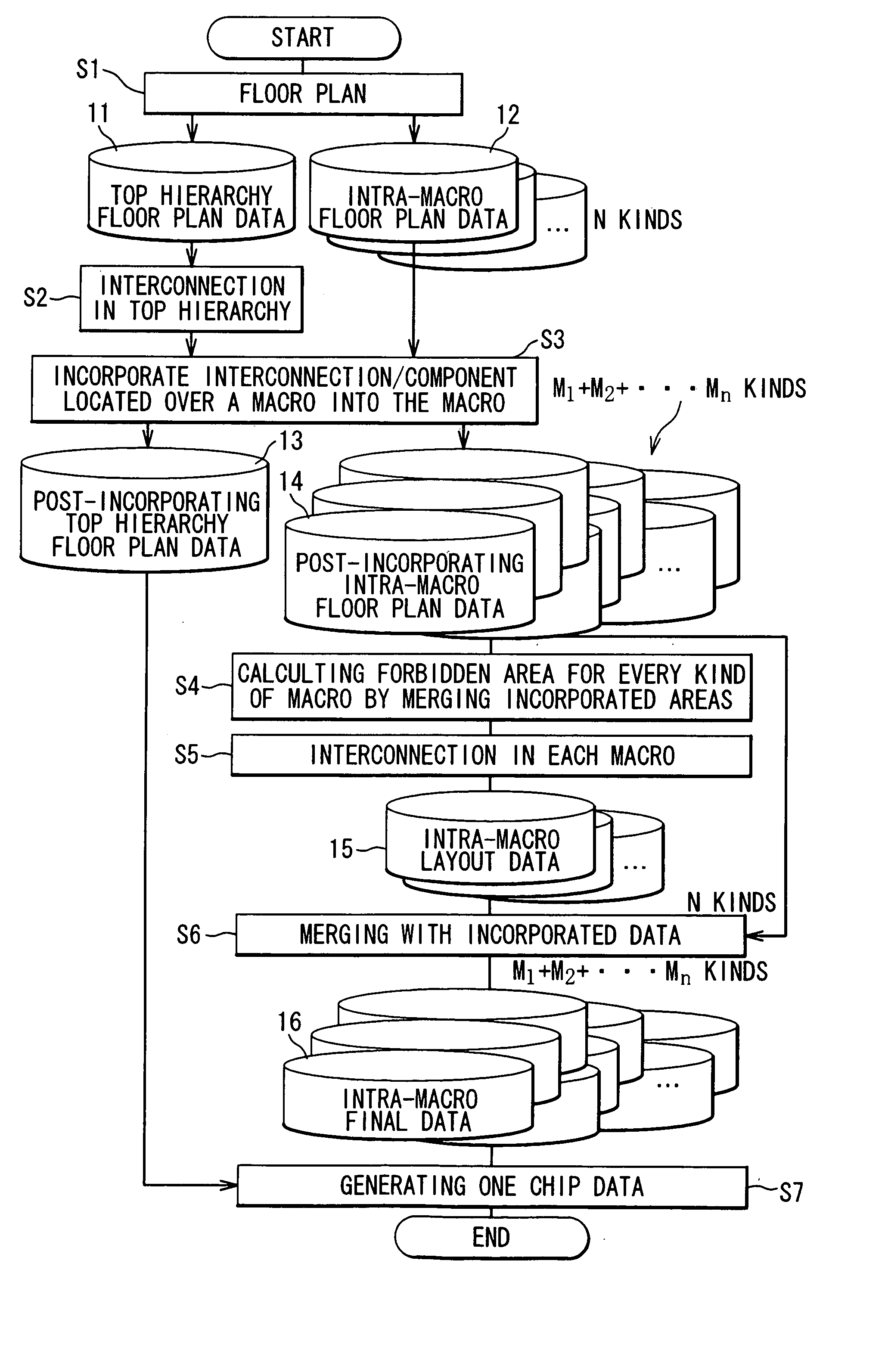
[0033]FIG. 3 is a flowchart showing a procedure of a method of laying-out a semiconductor device according to the present invention. First, a layout hierarchy is determined, and a netlist is divided based on the hierarchy ...


PUM


Abstract

A software product for laying-out a semiconductor device includes the functions of: (A) locating a plurality of macros including a plurality of first macros of the same kind belonging to a first hierarchy; (B) arranging interconnections connecting between the plurality of macros; (C) extracting from the interconnections a plurality of overlapping sections which overlap with the plurality of first macros, respectively; (D) incorporating respective of the overlapping sections into the first macros; (E) calculating a forbidden area associated with any overlapping section by superposing the plurality of overlapping sections with reference to orientations of the first macros; and (F) arranging interconnections / components belonging to a lower hierarchy within each first macro such that the interconnections / components are not provided in the forbidden area.

Description

BACKGROUND OF THE INVENTION [0001] 1. Field of the Invention [0002] The present invention relates to a software product for and a method of laying-out (designing) a semiconductor device. More particularly, the present invention relates to a software product for and a method of laying-out a semiconductor device by using a hierarchical design method. [0003] 2. Description of the Related Art In recent years, in the field of a semiconductor device such as a system LSI and an ASIC, the increase in required functions and performances makes the circuit configuration more complex. A hierarchical design method is often employed to design a semiconductor device. According to the hierarchical design method, a semiconductor device is treated as a set of function blocks (modules), and each of the function blocks is treated as a set of small-scale modules. Thus, a hierarchy structure is established. In the top hierarchy according to the hierarchical design, mega macros (large-scale function block...

Claims


Application Information

Patent Timeline
Patent Type & Authority Applications(United States)
IPC IPC(8): G06F17/50H01L21/82H01L21/822H01L27/04
CPCG06F17/5068G06F30/39H01L27/0207
Inventor ISHIZUKA, MICHI
Owner NEC ELECTRONICS CORP
Why Eureka
Try Eureka