
On-chip frequency degradation compensation

a technology of on-chip frequency degradation and compensation, applied in the field of on-chip testing, can solve the problems of low probability, low efficiency, and low resistance of the semiconductor integrated circuit, and achieve the effects of reducing the probability of transistor degradation, and reducing the efficiency of the semiconductor integrated circui

Active Publication Date: 2005-06-30
INTEL CORP
View PDF6 Cites 53 Cited by
  • Summary
  • Abstract
  • Description
  • Claims
  • Application Information

AI Technical Summary

Problems solved by technology

Over time, a semiconductor integrated circuit may become aged and experience higher resistances and lower drive capabilities in its transistors.
However, not all integrated circuits age in accordance with experiments performed during process development.
There is still a small probability that new integrated circuits, with a guard banded frequency rating, will fail as they age.
That is, these circuits may fail because they experience greater than expected aging.
A typical consumer integrated circuit may last seven years, at which point, one percent of their cumulative totals may have experienced catastrophic failure due to the unexpected degradation of their maximum operating frequencies, Fmax.
In this case, guard banding the frequency of the integrated circuit to a rated operating frequency is inefficient, as lower than expected aging may occur.
These new integrated circuits are never utilized to the extent of their capabilities.

Method used


Image

  • On-chip frequency degradation compensation
  • On-chip frequency degradation compensation
  • On-chip frequency degradation compensation

Examples


Embodiment Construction

[0014] In the following detailed description of embodiments of the invention, numerous specific details are set forth in order to provide a thorough understanding of the invention. However, it will be obvious to one skilled in the art that the embodiments of the invention may be practiced without these specific details. In other instances well known methods, procedures, components, and circuits have not been described in detail so as not to unnecessarily obscure aspects of the embodiments of the invention.

[0015] A compensation circuit adjusts the core clock frequency of an integrated circuit to account for real time frequency degradation due to transistor drive current reduction as time passes. By adjusting the core clock frequency of the integrated circuit, product failure may be avoided. The transistor driver current reduces over time as an integrated circuit is used due to known phenomenon caused by p-channel metal oxide semiconductor (PMOS) and n-channel metal oxide semiconduct...


PUM


Abstract

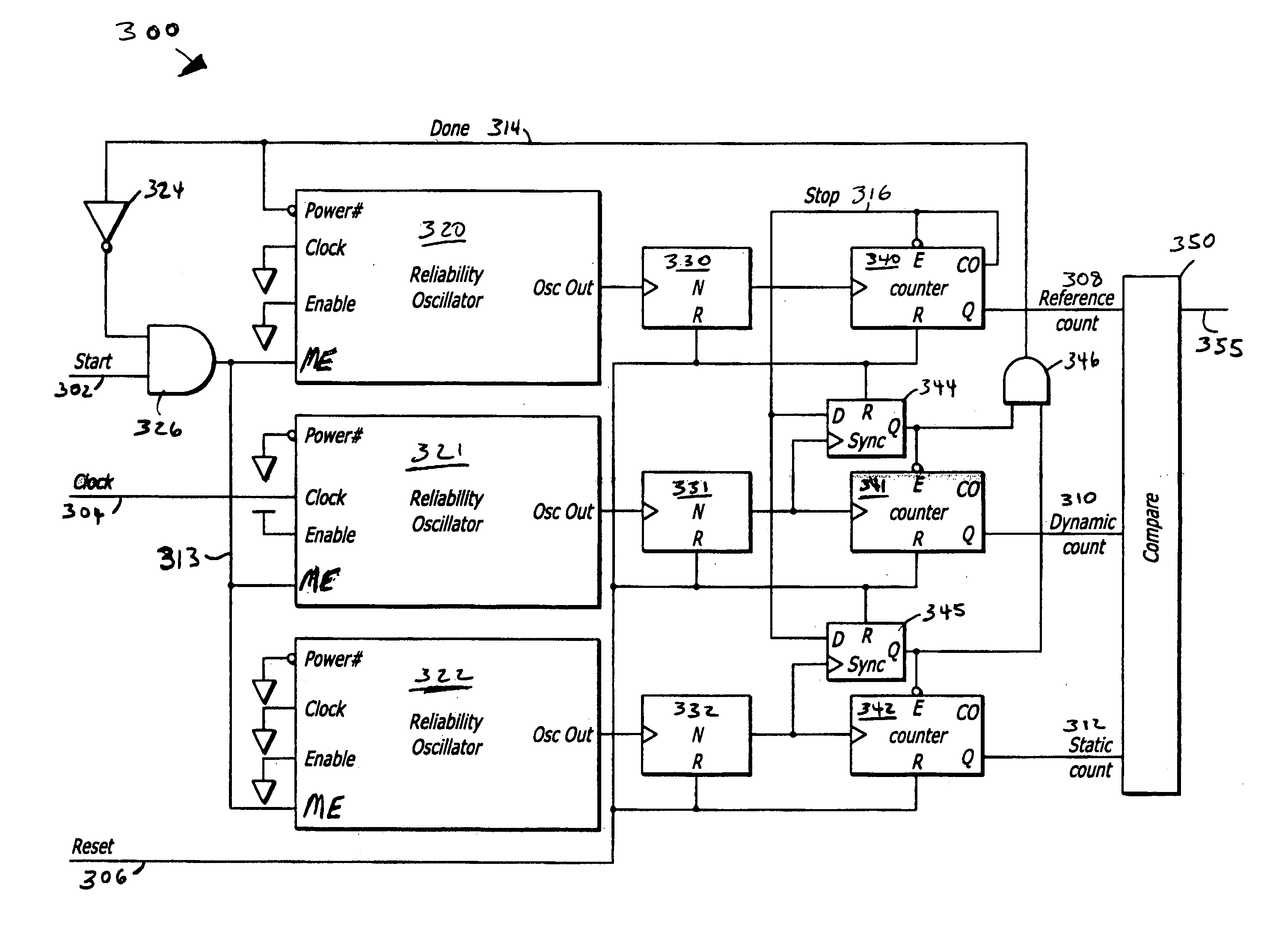
Embodiments of the invention include a trio of reliability oscillators. In one embodiment, an on-chip frequency compensation circuit includes a selectively enabled reliability oscillator to generate a reference oscillating signal, a clocked reliability oscillator to generate an AC degraded oscillating signal, and a static reliability oscillator to generate a DC bias degraded oscillating signal. A compare circuit coupled to the reliability oscillators compares the oscillating signals and generates a frequency compensation signal if the comparison determines that there is frequency degradation greater than a predetermined threshold.

Description

FIELD OF THE INVENTION [0001] Embodiments of the invention relate generally to on chip testing for integrated circuit reliability and quality assurance, and specifically to on-chip clock frequency compensation for transistor degradation. BACKGROUND OF THE INVENTION [0002] Over time, a semiconductor integrated circuit may become aged and experience higher resistances and lower drive capabilities in its transistors. These effects have become more pronounced as semiconductor integrated circuits have been scaled down. [0003] To compensate for the aging effects, a frequency guard band has been used during testing of a new integrated circuit that was recently manufactured. That is, the integrated circuit is tested to operate with a clock rate at a percentage guard band (GB) above the rated frequency. The percentage GB is predetermined through experiments performed during process development. In this manner if the integrated circuit ages accordingly, it has a higher operating probability o...

Claims


Application Information

Patent Timeline
IPC IPC(8): G06F1/04
CPCG06F1/04
Inventor MUNIANDY, RAVISANGARTAYLOR, GREGORY F.AMINZADEH, PAYMAN
Owner INTEL CORP
Learn More