Pixel based machine for patterned wafers

a pixel-based machine and wafer technology, applied in the field of surface inspection of semiconductor wafers, can solve the problems of inability or useless further operation, and achieve the effect of shortening processing times

Inactive Publication Date: 2005-06-16
APPLIED MATERIALS INC
View PDF19 Cites 10 Cited by
  • Summary
  • Abstract
  • Description
  • Claims
  • Application Information

AI Technical Summary

Benefits of technology

[0033] The method and apparatus of the invention can be used “inline”, viz. is suitable to be integrated with the production process tool, using the same wafer handling and interface system, and can operate as an integrated particle monitor to provide a constant check of the wafers produced, and in this way will detect any irregularities or defects that may arise in the production line. Sometimes unforeseen phenomena may occur in the production line that are so far-reaching as to render its further operation impossible or useless. It is important to detect such phenomena, which may be termed “catastrophic”, as soon as possible, and this invention permits to do so. These inline checks are rendered possible for the first time in the art by the high speed of the pixel-based inspection method and the moderate cost and footprint of the apparatus.
[0061] In another variant, the surface of the wafer is partitioned into a number of zones, a number of scanning beams (preferably equal to said number of zones) is provided, each scanning beam being associated with one of said zones, the inspected wafer is so moved that each beam scans the wafer zone associated with it, and the light produced by the scattering of each beam by the wafer surface is collected in a plurality of fixed directions associated with said beam. Typically and preferably, said zones of the wafer, except the central one, which is circular, are annular, concentric rings having similar radial dimensions, and the wafer is rotated and is shifted approximately radially by an amount equal to said radial dimension of the rings. This variant of the invention shortens the processing times, requires smaller motions of the apparatus elements and permits to define smaller pixels.

Problems solved by technology

Sometimes unforeseen phenomena may occur in the production line that are so far-reaching as to render its further operation impossible or useless.

Method used


Image

  • Pixel based machine for patterned wafers
  • Pixel based machine for patterned wafers
  • Pixel based machine for patterned wafers

Examples


Embodiment Construction

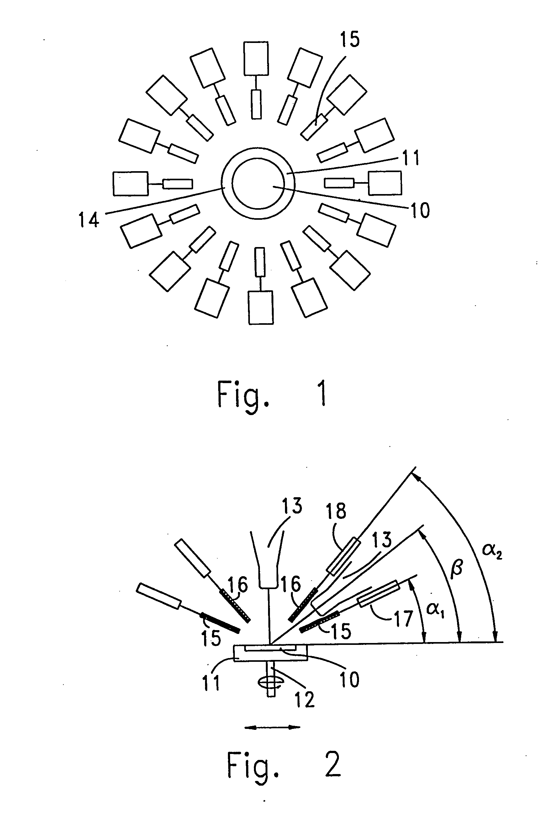
[0115]FIGS. 1 and 2 schematically represent an apparatus according to an embodiment of the invention. Numeral 10 indicates a wafer that is being inspected. The apparatus used for the inspection comprises a stage having a wafer support. The wafer is placed on said support, which in this embodiment is a support plate 11, which is rotated about shaft 12 by mechanical means, not shown as being conventional. A laser source is shown at 13 in its central position, above the axis of shaft 12. However, more than one source could be provided and any source could be placed at an angle to the axis of shaft 12, to provide the required illumination of the wafer, depending on the type of wafer under inspection. In FIG. 2 one such additional laser source is shown, by way of illustration, oriented at an angle β from the plane of the wafer. Mechanical means, not shown as being conventional, translate the shaft 12, viz. shift it, while maintaining it parallel to itself, so that any point thereof moves...


PUM

PropertyMeasurementUnit
wavelengthaaaaaaaaaa

Abstract

A method is provided for the detection of defects on a semiconductor wafer by checking individual pixels on the wafer, collecting the signature of each pixel, defined by the way in which it responds to the light of a scanning beam, and determining whether the signature is that of a faultless pixel or of a pixel that is defective or suspect to be defective. An apparatus is also provided for the determination of such defects, which comprises a stage for supporting a wafer, a laser source generating a beam that is directed onto the wafer, collecting optics and photoelectric sensors for collecting the laser light scattered by the wafer in a number of directions and generating corresponding analog signals, an A / D converter deriving from the signals digital components defining pixel signatures, and selection systems for identifying the signatures of suspect pixels and verifying whether the suspect pixels are indeed defective.

Description

FIELD OF THE INVENTION [0001] The invention relates to the inspection of surfaces, particularly the surfaces of semiconductor wafers, intended for the detection of possible defects, particularly due to the presence of particles. More particularly the invention relates to the control of semiconductor manufacturing processes, particularly Quality Control, Process Monitoring and Control and Catastrophe Detection. The invention further comprises method and apparatus for the inline control of wafer production and the immediate recognition of any fault or irregularities in the production line. BACKGROUND OF THE INVENTION [0002] The detection of defects and / or of the presence of foreign substances on semiconductor wafers has received considerable attention in the art. Defects can be caused by an imperfect production of the desired pattern. Further, particles of various kinds may adhere to a wafer surface for a number of reasons. [0003] The inspection process can be carried out on bare wafe...

Claims


Application Information

Patent Timeline
Patent Type & Authority Applications(United States)
IPC IPC(8): G01N21/88G01N21/956G01N21/94
CPCG01N21/94G01N21/9501G01N21/9505G01N2021/8893
Inventor SMILANSKY, ZEEVTSADKA, SAGIELAPIDOT, ZVISHERMAN, RIVI
Owner APPLIED MATERIALS INC
Why Eureka
Try Eureka