
Liquid crystal on silicon (LCOS) display device having a uniform cell gap

a liquid crystal and cell gap technology, applied in static indicating devices, instruments, optics, etc., can solve the problems of non-uniform luminance, image quality deterioration, resolution and luminance limitations of existing cathode ray tube projectors, etc., and achieve uniform cell gap

Inactive Publication Date: 2005-06-16
SAMSUNG ELECTRONICS CO LTD
View PDF26 Cites 22 Cited by
  • Summary
  • Abstract
  • Description
  • Claims
  • Application Information

AI Technical Summary

Benefits of technology

[0013] An exemplary aspect of the present invention is to provide provides an LCOS display device which alleviates, without requiring spacers, disadvantages due to uneven cell gap which may be generated during the manufacturing of the product or service of the product.
[0017] The LCOS display device achieves uniformity of the cell gap by adjusting the voltage level of the thin piezo-electric layer after bonding the wafer and the glass, and therefore, it is not required to use spacers. Also, when the wafer suffers from deformation due to heat or other reasons during the service of product, the deformation can also be compensated.

Problems solved by technology

Existing cathode ray tube (CRT) projectors have limitations in regard to resolution and luminance.
Also, a grid pattern appears in the LCD, causing the image quality deterioration.
If there is non-uniformity, then the transmittance of light that penetrates through the cell gap loses consistency, causing non-uniform luminance.
As a result, the cell gap does not have uniformity.
Also, even if the uniformity of the gap is maintained right after the manufacturing process, the cell gap may be deformed by the heat generated during the service of the product, which also causes the image quality deterioration.
Therefore, deterioration of the image quality is caused due to it being impossible to place the spacers during the manufacture of an LCOS display device, and therefore, there is a demand for the substitution for the conventional spacers.

Method used


Image

  • Liquid crystal on silicon (LCOS) display device having a uniform cell gap
  • Liquid crystal on silicon (LCOS) display device having a uniform cell gap
  • Liquid crystal on silicon (LCOS) display device having a uniform cell gap

Examples


Embodiment Construction

[0023] Hereinafter, exemplary embodiments of the present invention will be described in detail with reference to the accompanying drawings.

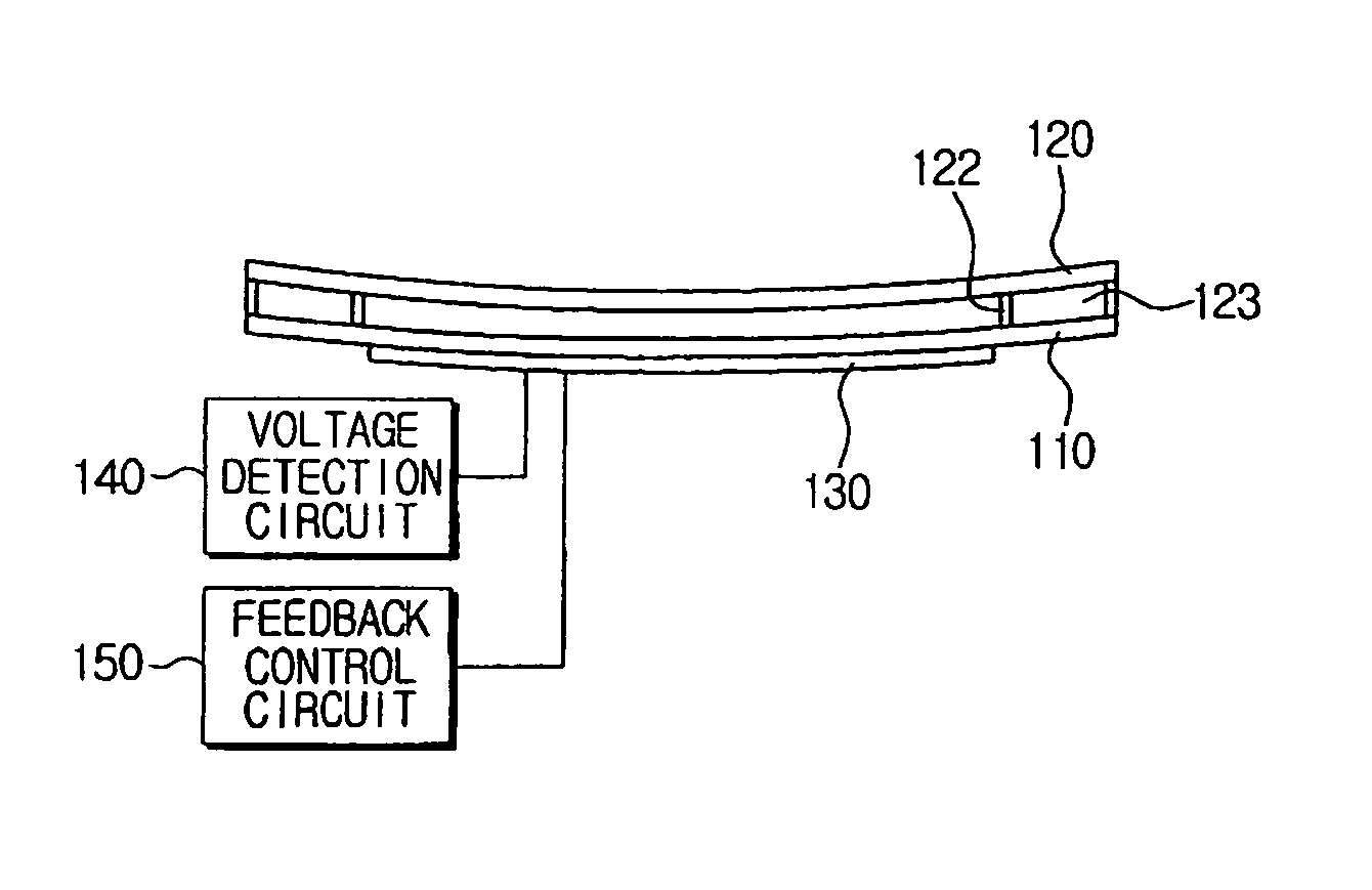
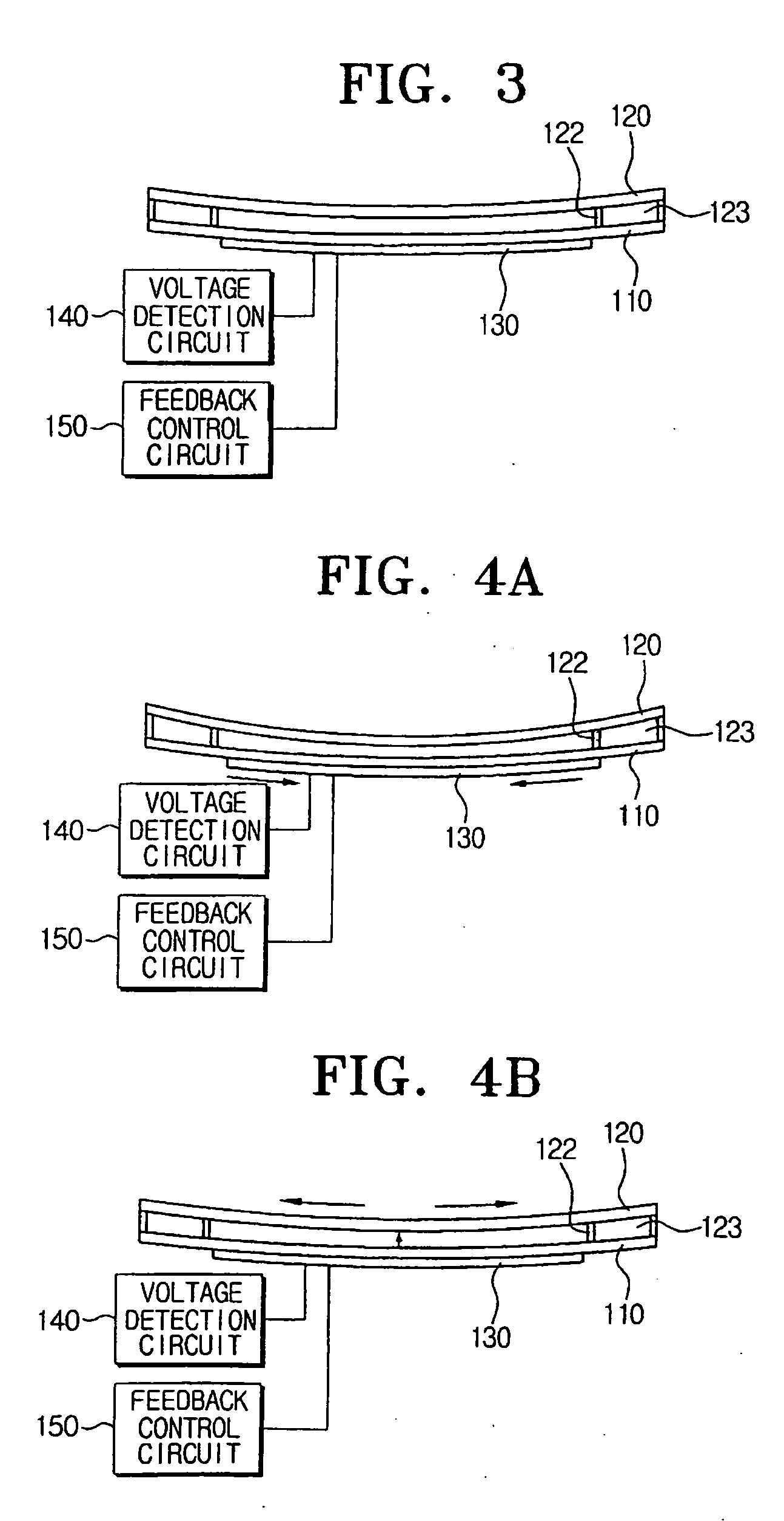
[0024]FIG. 3 is a cross section view showing an LCOS display device according to an exemplary embodiment of the present invention. Referring to FIG. 3, the LCOS display device comprises a wafer 110, a glass 120, walls 122 containing sealant 123, and a thin piezo-electric layer 130. Although not shown, an electrode is further provided in the LCOS display device to connect the thin piezo-electric layer 130 to an external power source.

[0025] The thin piezo-electric layer 130 is made from a material that generates an electric charge under the pressure, and contracts and / or expands when being applied with a voltage. It is common knowledge that the thin piezo-electric layer 130 has been already used in fine ink particle-jetting of an ink jet printer. Therefore, the thin piezo-electric layer 130 is feasible to the manufacturing of an LCOS display devi...


PUM


Abstract

A liquid crystal on silicon (LCOS) device includes a wafer, glass, and walls formed at opposite ends of an upper surface of the wafer to define a predetermined cell gap between the glass and the wafer. A thin piezo-electric layer is attached onto a surface of the wafer and an electrode is applied with external power to expand and / or contract the thin piezo-electric layer. The LCOS device further includes a voltage detection unit for detecting a voltage generated by the deformation of the thin piezo-electric layer; and a feedback control unit for compensating for deformation of the thin piezo-electric layer according to the voltage detected by the voltage detection unit. The LCOS device achieves uniformity of the cell gap by adjusting the voltage level of the thin piezo-electric layer after bonding the wafer and the glass, and therefore, spacers are not required.

Description

CROSS-REFERENCE TO RELATED APPLICATIONS [0001] This application claims priority from Korean Patent Application No. 2003-91440, filed Dec. 15, 2003, in the Korean Intellectual Property Office, the disclosure of which is incorporated herein by reference. BACKGROUND OF THE INVENTION [0002] 1. Field of the Invention [0003] Apparatuses and methods consistent with the present invention relate to a display device, and in particular but not exclusively, relate to a liquid crystal on silicon (LCOS) display device having pixel arrays on a silicon wafer. [0004] 2. Description of the Related Art [0005] The age of multimedia has arrived, and a user's demand for large-sized display devices is appreciably increasing, which accelerates the development of the large-sized display devices. Existing cathode ray tube (CRT) projectors have limitations in regard to resolution and luminance. This shortcoming has been offset by recently developed liquid crystal display (LCD) projectors or digital light proc...

Claims


Application Information

Patent Timeline
IPC IPC(8): G02F1/1339G02F1/133G02F1/1333G02F1/1362H01L41/08
CPCG02F1/1333G02F1/133305G02F1/136277G02F2001/133368G02F2203/18G02F1/133368G02F1/1339
Inventor BOOH, SEONG-WOONSHIN, SU-HOKIM, SU-GUNCHO, JIN-WOOWANG, JONG-MIN
Owner SAMSUNG ELECTRONICS CO LTD
Learn More