A/D converter apparatus and D/A converter apparatus
- Summary
- Abstract
- Description
- Claims
- Application Information
AI Technical Summary
Benefits of technology
Problems solved by technology
Method used
Image
Examples
first embodiment
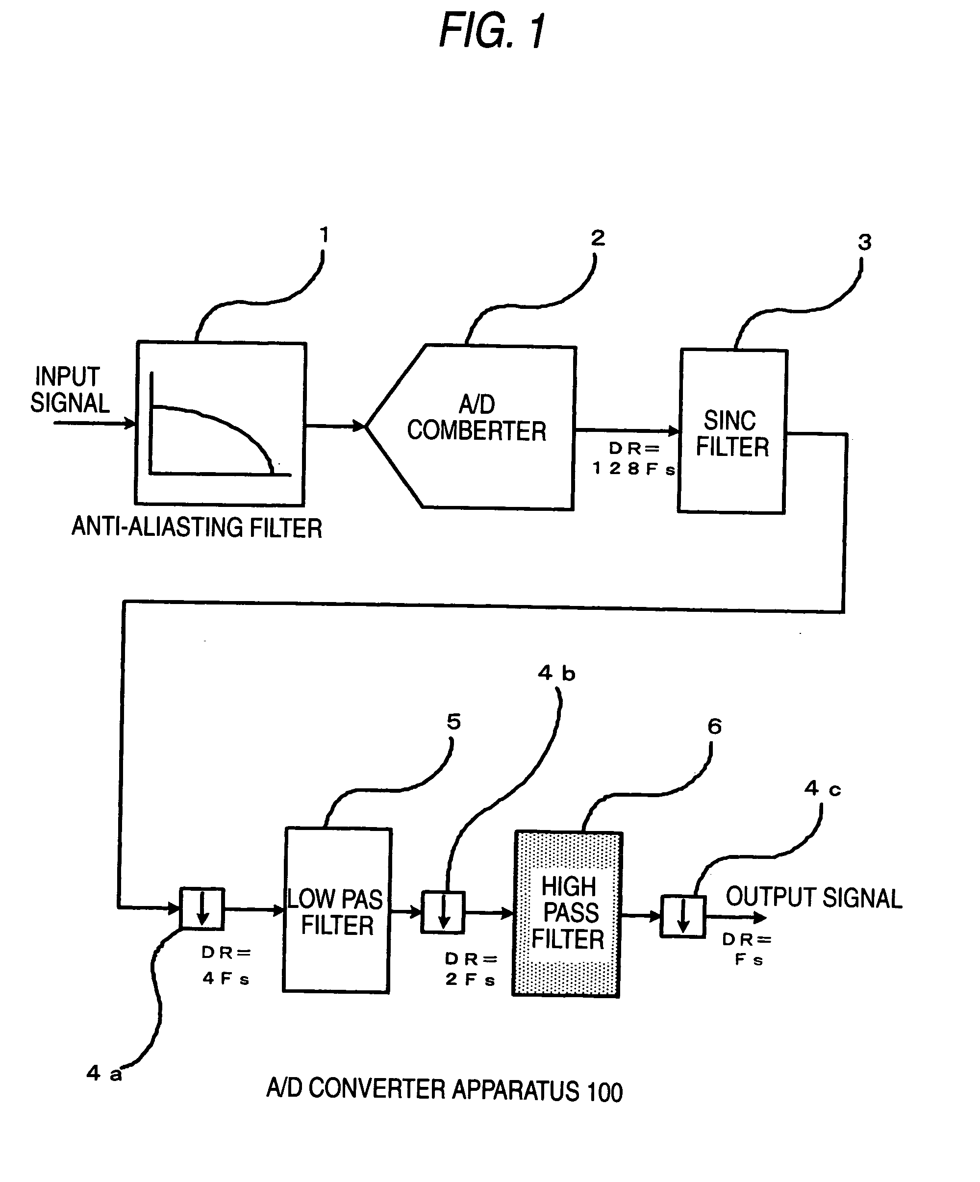
[0033]FIG. 1 is a block diagram showing a schematic structure of an A / D converter apparatus 100 according to a first embodiment of the present invention. The A / D converter apparatus 100 comprises an anti-aliasing filter 1 for previously removing an aliasing noise generated by sampling, an A / D converter 2 for converting an analog signal into a digital signal at a sampling rate of 128Fs (Fs is the data rate of the digital signal which is desired to be obtained), a SINC filter (comb filter) 3 for removing an aliasing noise due to down-sampling, a first decimator 4a for performing down-sampling at the data rate of DR=4Fs, a low pass filter 5 for removing an aliasing noise due to down-sampling, a second decimator 4b for performing down-sampling at the data rate of DR=2Fs, a high pass filter 6 for removing a DC component from a signal output from the decimator 4b, and a third decimator 4c for down-sampling a signal output from the high pass filter 6 at the data rate of DR=Fs.
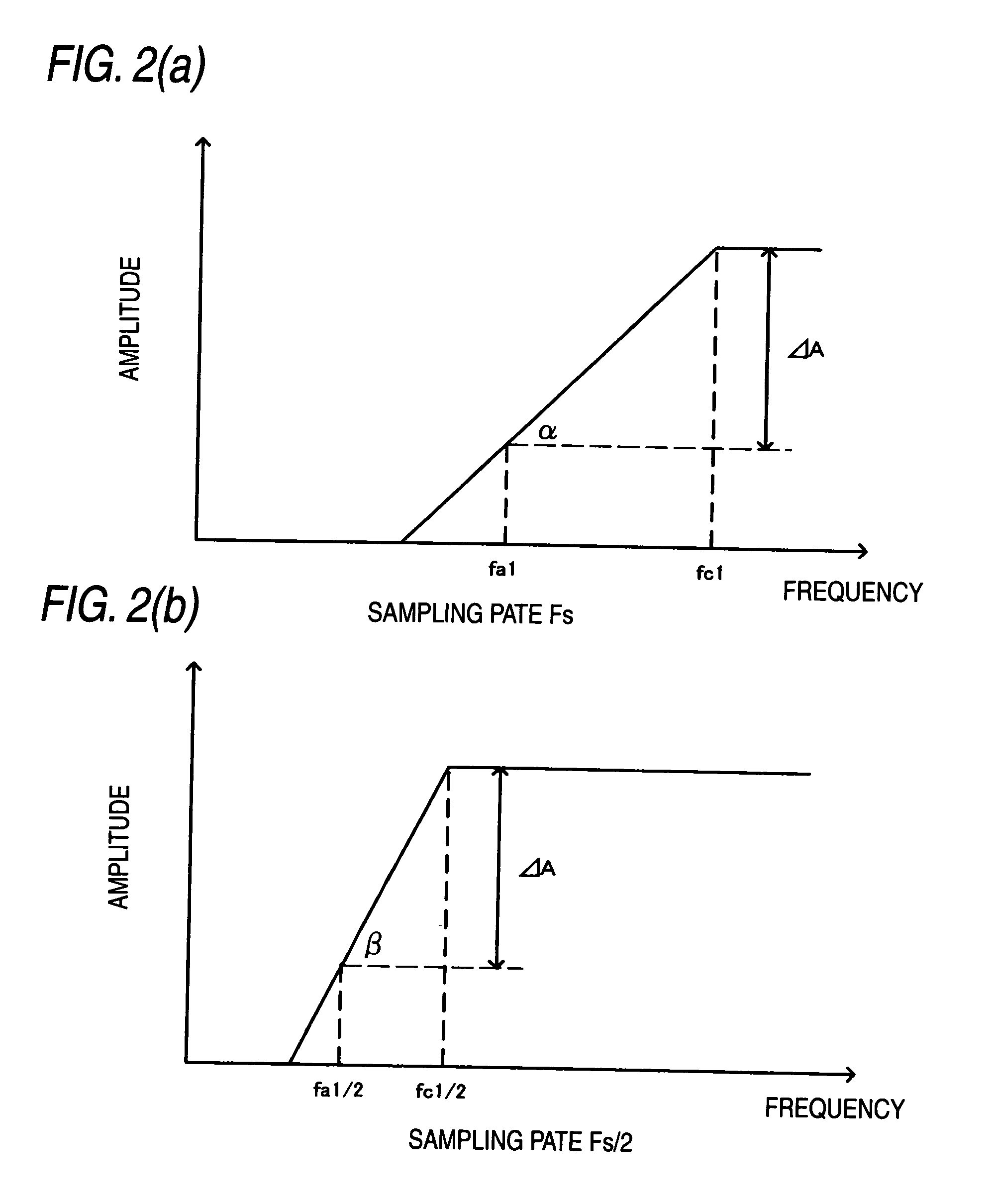
[0034] The a...
second embodiment
[0045]FIG. 3 is a block diagram showing a schematic structure of a D / A converter apparatus 200 of a second embodiment of the present invention. The D / A converter apparatus 200 comprises a first interpolator 7a for increasing the data rate of a digital input signal to 2Fs, a high pass filter 6 for removing a DC component, similar to the first embodiment, a second interpolator 7b for increasing the data rate thereof to 4Fs, a first low pass filter 5 for removing the spectrum at 2Fs, 3Fs among the spectrums of the digital input signal which are repeated at the interval of Fs and allowing the spectrum to be repeated for each 4Fs, a third interpolator 7c for increasing the data rate to 128Fs, a second low pass filter 8 for removing the spectrum which exists at the interval of 4Fs, a D / A converter 9 for converting the digital signal into an analog signal, and a smoothing filter 10 for removing an aliasing spectrum shifted to the band of 128Fs by the third interpolator 7c and extracting on...
third embodiment
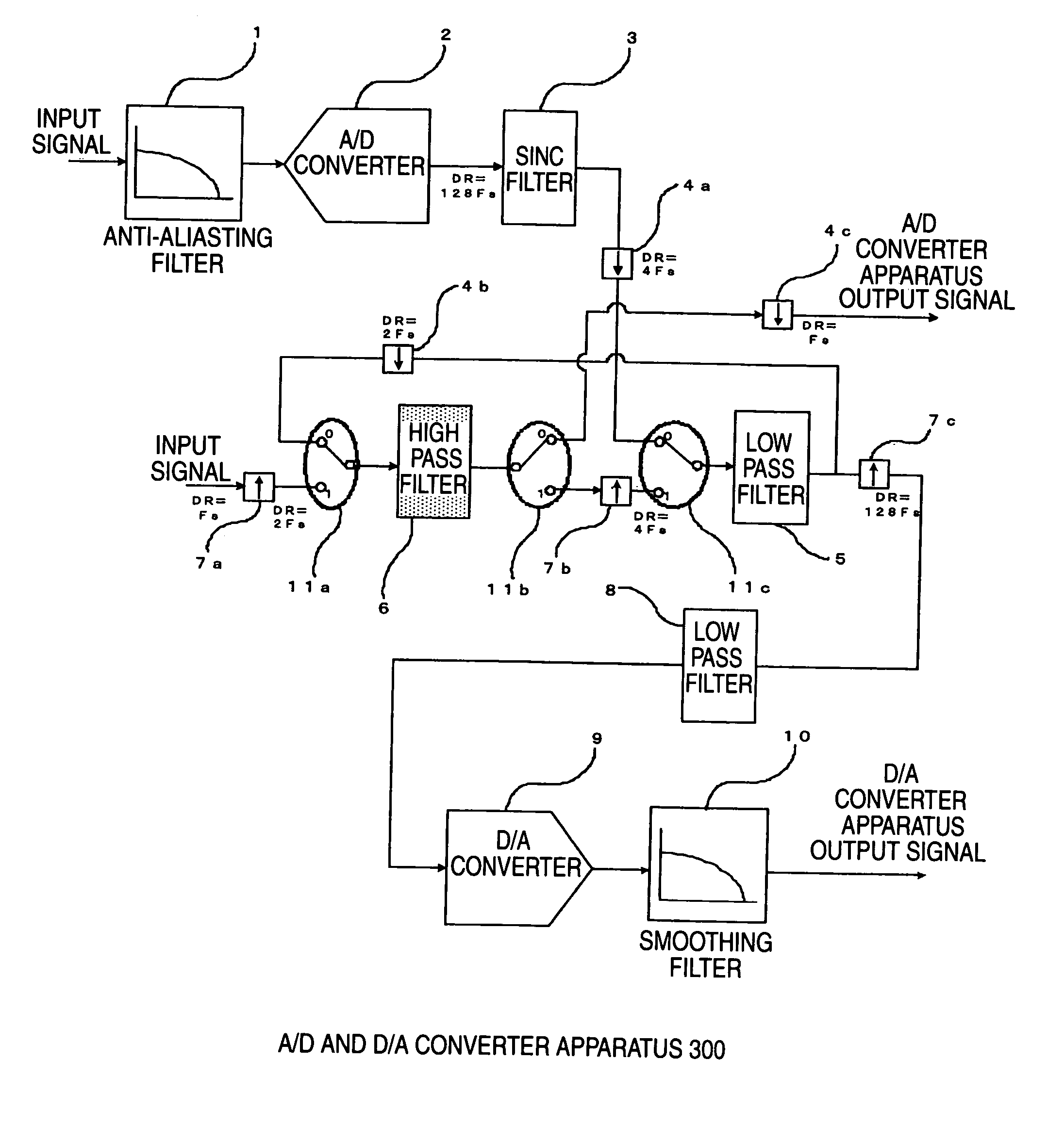
[0047]FIG. 4 is a block diagram showing a schematic structure of an A / D and D / A converter apparatus 300 composed by combining the A / D converter apparatus 100 described in the first embodiment and the D / A converter apparatus 200 described in the second embodiment. The A / D and D / A converter apparatus 300 of the present embodiment comprises an anti-aliasing filter 1, an A / D converter 2, a SINC filter (comb filter) 3, first to third decimators 4a, 4b, and 4c, a first low pass filter 5, a high pass filter 6, first to third interpolators 7a, 7b, and 7c, a second low pass filter 8, a D / A converter 9, a smoothing filter 10, and first to third switches 11a, 11b, and 11c each having a terminal A and a terminal B which are switched in response to a control signal as a sharing means for switching data paths for A / D conversion and D / A conversion.
[0048] The functions of the components are equal to that described in the first and second embodiments. The A / D and D / A converter apparatus 300 functio...
PUM
 Abstract
Description
Claims
Application Information
 - R&D
- Intellectual Property
- Life Sciences
- Materials
- Tech Scout
- Unparalleled Data Quality
- Higher Quality Content
- 60% Fewer Hallucinations
Browse by: Latest US Patents, China's latest patents, Technical Efficacy Thesaurus, Application Domain, Technology Topic, Popular Technical Reports.
© 2025 PatSnap. All rights reserved.Legal|Privacy policy|Modern Slavery Act Transparency Statement|Sitemap|About US| Contact US: help@patsnap.com


