
Methods of nanotubes films and articles

a technology of carbon nanotubes and films, applied in the direction of discharge tubes luminescnet screens, semiconductor/solid-state device details, instruments, etc., can solve the problems of non-continuous, inconvenient use, and inability to meet the needs of electrical interconnects in semiconductor devices, etc., and achieve the effect of nanotube growth

Inactive Publication Date: 2005-05-12
ZEON CORP
View PDF98 Cites 286 Cited by
  • Summary
  • Abstract
  • Description
  • Claims
  • Application Information

AI Technical Summary

Benefits of technology

The invention provides methods for making nanotube films and articles with conductive properties. The methods involve growing nanotube segments on a substrate to form a network of nanotubes. The nanotube segments can be single or multi-walled carbon nanotubes, and may have different lengths. The nanotube fabric can be formed on the substrate using a gas phase catalyst or a metallic gas phase catalyst. The nanotube fabric can also be deposited on the substrate by depositing a solution of suspended nanotubes or by spraying an aerosol with nanotubes onto the surface of the substrate. The invention also provides a method for making conductive articles on a substrate by patterning a nanotube fabric on the substrate and removing a portion of the fabric to form conductive articles. The patterned layer can be an insulator or a semiconductor, and the nanotubes grow in areas other than the patterned metal layer. The technical effects of the invention include the ability to make conductive nanotube films and articles with precise control over their structure and properties.

Problems solved by technology

Metal films in this size regime are usually non-continuous and not conductive over macroscopic distances.
Furthermore, these sub-10 nm films are prone to thermal damage by electrical current making them unsuitable for applications such as electrical interconnects in semiconductor devices.
Conventional interconnect technologies have a tendency to suffer from thermal damage and metal diffusion eroding the performance of the semiconductor devices especially from degradation of the electrical properties.

Method used


Image

  • Methods of nanotubes films and articles
  • Methods of nanotubes films and articles
  • Methods of nanotubes films and articles

Examples


Embodiment Construction

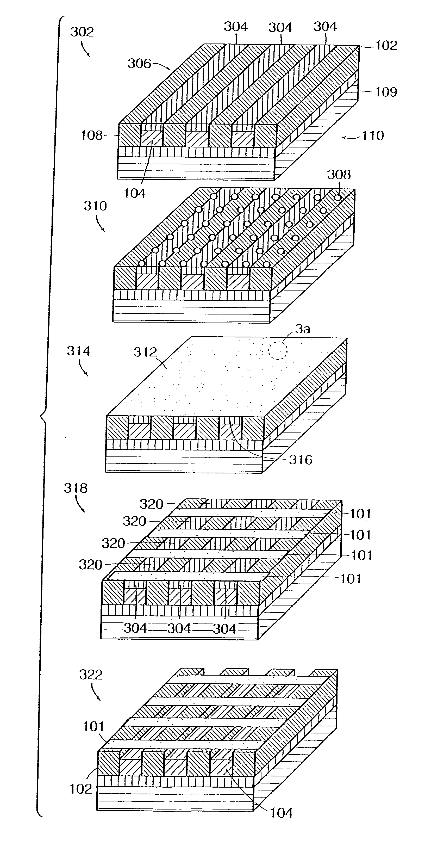
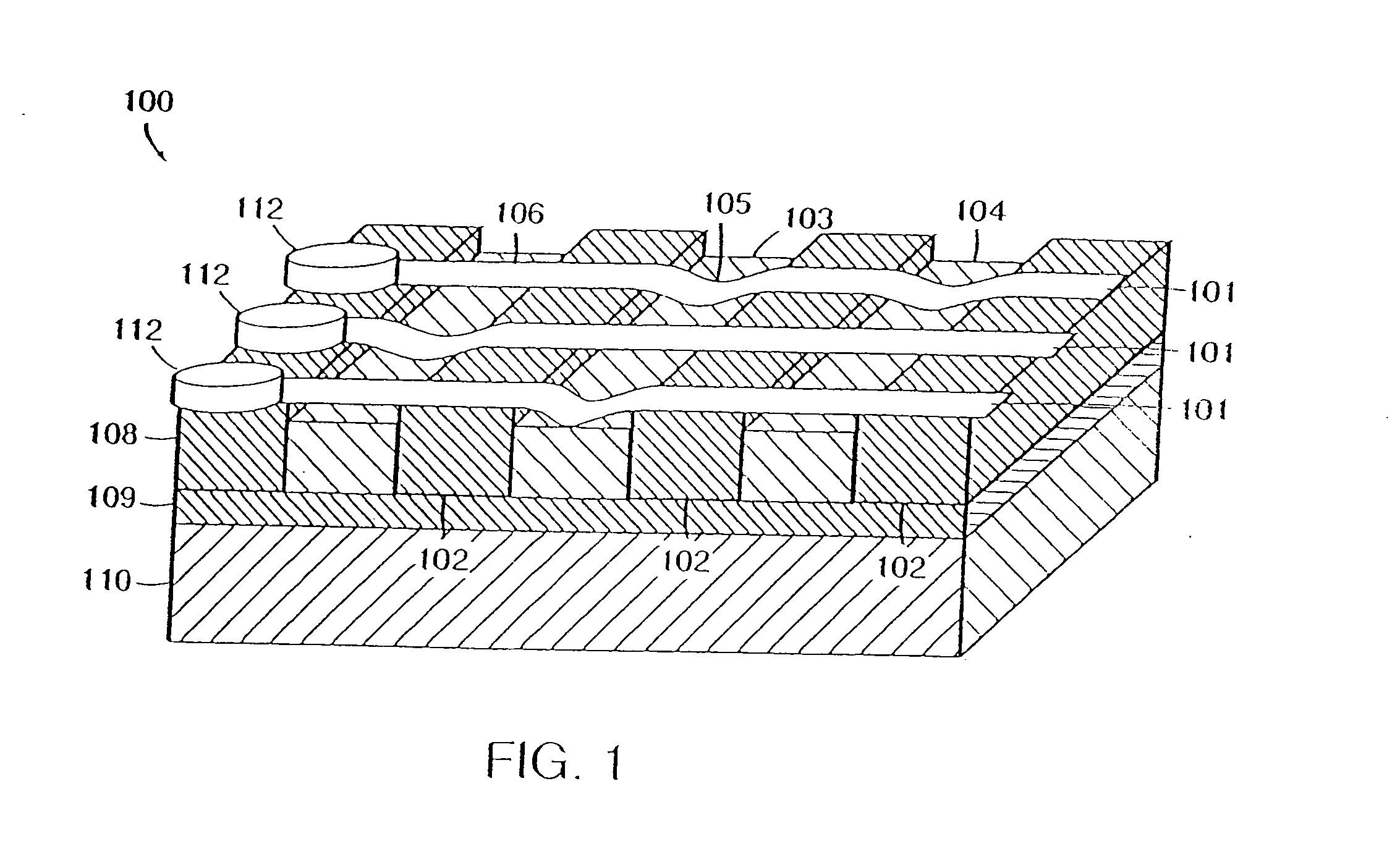
[0039] New electromechanical memory arrays and methods for making same are disclosed in which electromechanical memory cells are created that operate analogously to the NTWCM devices disclosed in WO 01 / 03208, which is hereby incorporated by reference in its entirety. However, unlike the NTWCM devices disclosed in WO 01 / 03208, new ribbons or belts made from a matted layer of nanotubes or a non-woven fabric of nanotubes are used as an electrically conductive element. At points in this disclosure, the ribbons are referred to as traces or electrically conductive articles. In some instances, the ribbons are suspended, and in other instances they are disposed on a substrate. In some instances, they are used to deflect to certain states under electrical control, and in other instances they do not move and instead are used simply to carry an electrical current or voltage. The new nanotube belt structures are believed to be easier to build at the desired levels of integration and scale (in n...


PUM

PropertyMeasurementUnit
diametersaaaaaaaaaa
widthaaaaaaaaaa
temperatureaaaaaaaaaa

Abstract

Nanotube films and articles and methods of making the same are disclosed. A conductive article includes an aggregate of nanotube segments in which the nanotube segments contact other nanotube segments to define a plurality of conductive pathways along the article. The nanotube segments may be single walled carbon nanotubes, or multi-walled carbon nanotubes. The various segments may have different lengths and may include segments having a length shorter than the length of the article. The articles so formed may be disposed on substrates, and may form an electrical network of nanotubes within the article itself. Conductive articles may be made on a substrate by forming a nanotube fabric on the substrate, and defining a pattern within the fabric in which the pattern corresponds to the conductive article. The nanotube fabric may be formed by growing the nanotube fabric on the substrate using a catalyst, for example, in which the catalyst is a gas phase catalyst, or in which the catalyst is a metallic gas phase catalyst. The nanotube fabric may be formed by depositing a solution of suspended nanotubes on the substrate. The deposited solution may be spun to create a spin-coating of the solution. The solution may be deposited by dipping the substrate into the solution. The nanotube fabric is formed by spraying an aerosol having nanotubes onto a surface of the substrate.

Description

CROSS-REFERENCE TO RELATED APPLICATIONS [0001] This application is a continuation of U.S. patent application Ser. No. 10 / 128117, filed Apr. 23, 2002, entitled Methods of Nanotube Films and Articles, which is a continuation-in-part of U.S. patent application Ser. No. 09 / 915093, filed Jul. 25, 2001, entitled Electromechanical Memory Array Using Nanotube Ribbons and Method for Making Same, U.S. patent application Ser. No. 09 / 915173, filed Jul. 25, 2001, now U.S. Pat. No. 6,643,165, entitled Electromechanical Memory Having Cell Selection Circuitry Constructed with Nanotube Technology; and U.S. patent application Ser. No. 09 / 915095, filed Jul. 25, 2001, now U.S. Pat. No. 6,574,130, entitled Hybrid Circuit Having Nanotube Electromechanical Memory, all of which are incorporated herein by reference in their entirety.BACKGROUND [0002] 1. Technical Field [0003] This invention relates in general to carbon nanotube films, fabrics, layers, and articles and in particular to making electrically co...

Claims


Application Information

Patent Timeline
Patent Type & Authority Applications(United States)
IPC IPC(8): B82B1/00B81B3/00G11C13/02G11C23/00H01L21/3205H01L21/768H01L23/52H01L27/10H01L27/12H01L27/24H10K99/00
CPCB82Y10/00Y10S977/857G11C23/00G11C2213/16G11C2213/77G11C2213/81H01H1/0094H01L21/76838H01L27/10H01L27/1203H01L51/0048H01L51/444H01L29/413Y10S977/888Y10S977/75Y10S977/843Y10S977/778G11C13/025H01L2221/1094H10K85/221H10K30/821H10B99/10B82B1/00
Inventor RUECKES, THOMASSEGAL, BRENT M.
Owner ZEON CORP
Learn More