Switching power source circuit
- Summary
- Abstract
- Description
- Claims
- Application Information
AI Technical Summary
Benefits of technology
Problems solved by technology
Method used
Image
Examples
first embodiment
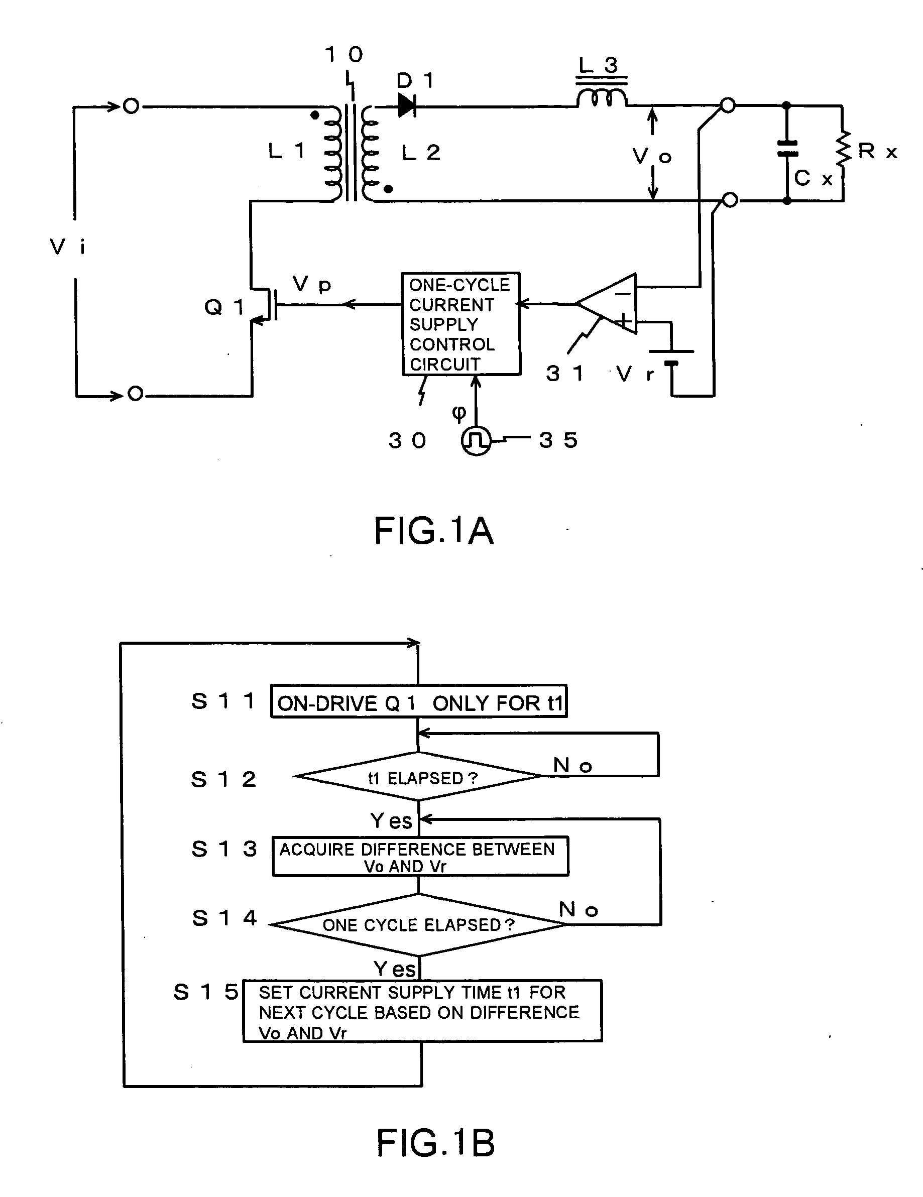
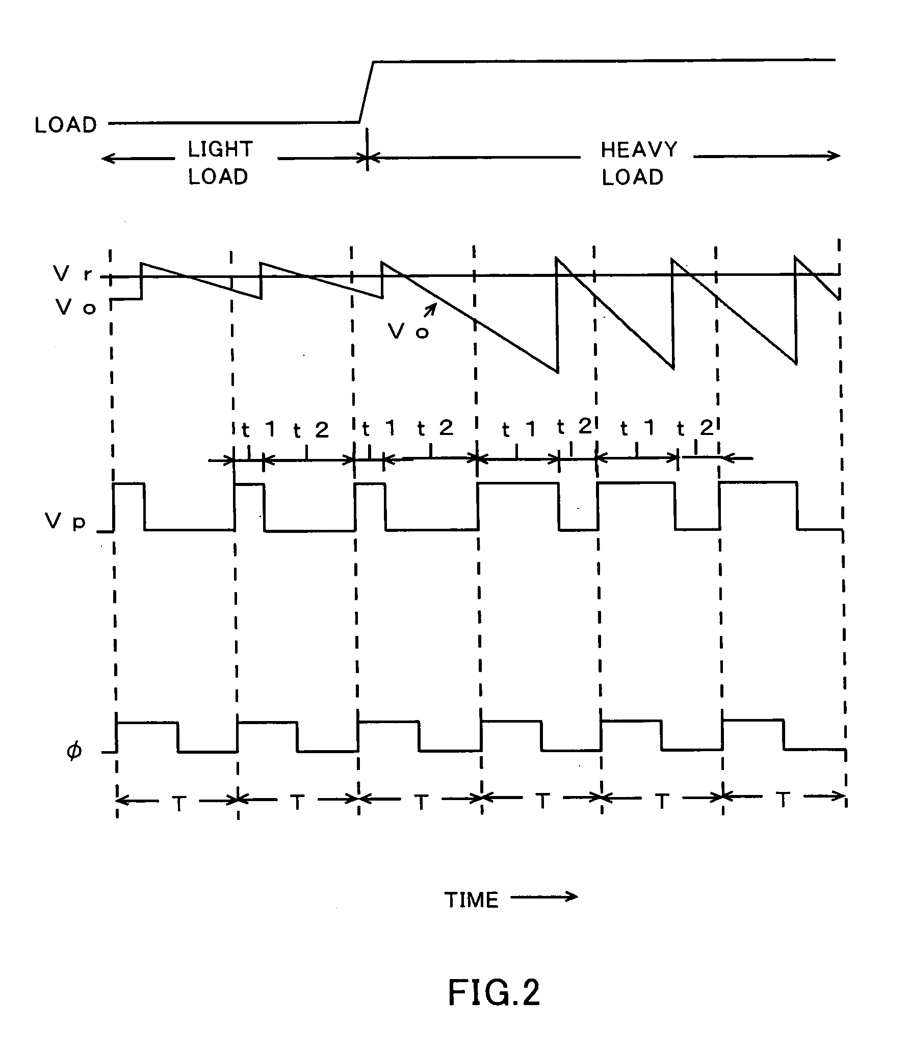
[0036]FIGS. 1A and 1B illustrate a switching power supply circuit according to the present invention. FIG. 1A shows a circuit diagram of a principal part of the switching power supply circuit, and FIG. 1B shows a flow chart illustrating an operation of the principal part thereof. FIG. 2 shows a waveform chart illustrating an operation in the principal part of the circuit of FIG. 1A.
[0037] The switching power supply circuit illustrated in the figures is constituted with use of a power MOS transistor Q1 as a switching element, a high frequency power transformer 10, a diode D1, a choke coil L3, a one-cycle current supply control circuit 30 serving also as a driving circuit for the switching element, a voltage comparison circuit 31, a clock generator 35, and the like as shown in FIG. 1A. In this case, the choke coil L3 is equivalently formed by an inductance which is not coupled to a power transformer, and an inductance distributed or parasitized on a current line or the like.
[0038] In...
second embodiment
[0044]FIGS. 3A show the switching power supply circuit according to the present invention. FIG. 3A shows a circuit diagram of a principal part thereof, and FIG. 3B shows a waveform chart of an operation thereof.
[0045] This second embodiment is a more specified example of the foregoing first embodiment, and an integration circuit 33 and a single pulse with-variable-width generator 34 are used in order to constitute the foregoing one-cycle current supply control circuit 30.
[0046] The voltage comparison circuit 31 for detecting a control error outputs a difference between an output voltage Vo and a reference voltage Vr in the form of a binary logic level of high and low levels. Specifically, when the output voltage Vo, that is, a control value, falls below the reference voltage Vr, that is, a target value, the voltage comparison circuit 31 outputs an active level of high. When the output voltage Vo exceeds the reference voltage Vr, the comparison circuit 31 outputs an inactive level o...
third embodiment
[0048]FIGS. 4A and 4B show the present invention. Respectively, FIG. 4A shows a circuit diagram of a principal part thereof, and FIG. 4B shows a waveform chart of an operation thereof.
[0049] A switching power supply circuit of the third embodiment is constituted so that while an input current, which is supplied thereto at the time when a power MOS transistor Q1 is made to be turned on, is accumulated in a coil L4, an inertial current (shown by the dotted line with arrow) flowing through the coil L4 at the time when the transistor is made to be turned off is rectified by a diode D1 to be charged in a capacitor C1, whereby an output voltage Vo is taken out from the capacitor C1. A so-called back converter-type switching power supply circuit is constituted.
[0050] In this embodiment, as in the case of the foregoing second embodiment, a current supply time t1 of each current supply cycle T is variably set with use of a voltage comparison circuit 31 which outputs a difference between an ...
PUM
 Abstract
Description
Claims
Application Information
 - R&D
- Intellectual Property
- Life Sciences
- Materials
- Tech Scout
- Unparalleled Data Quality
- Higher Quality Content
- 60% Fewer Hallucinations
Browse by: Latest US Patents, China's latest patents, Technical Efficacy Thesaurus, Application Domain, Technology Topic, Popular Technical Reports.
© 2025 PatSnap. All rights reserved.Legal|Privacy policy|Modern Slavery Act Transparency Statement|Sitemap|About US| Contact US: help@patsnap.com


