Overlay mark for aligning different layers on a semiconductor wafer
a technology of overlay marks and semiconductor wafers, applied in the field of overlay marks, can solve the problems of not meeting the requirements of the client, erroneous measurement of specifications, and the alignment between the pattern of the pre-layer and the pattern of the photoresist layer will not meet the accuracy requirements, so as to save the area cost
- Summary
- Abstract
- Description
- Claims
- Application Information
AI Technical Summary
Benefits of technology
Problems solved by technology
Method used
Image
Examples
first embodiment
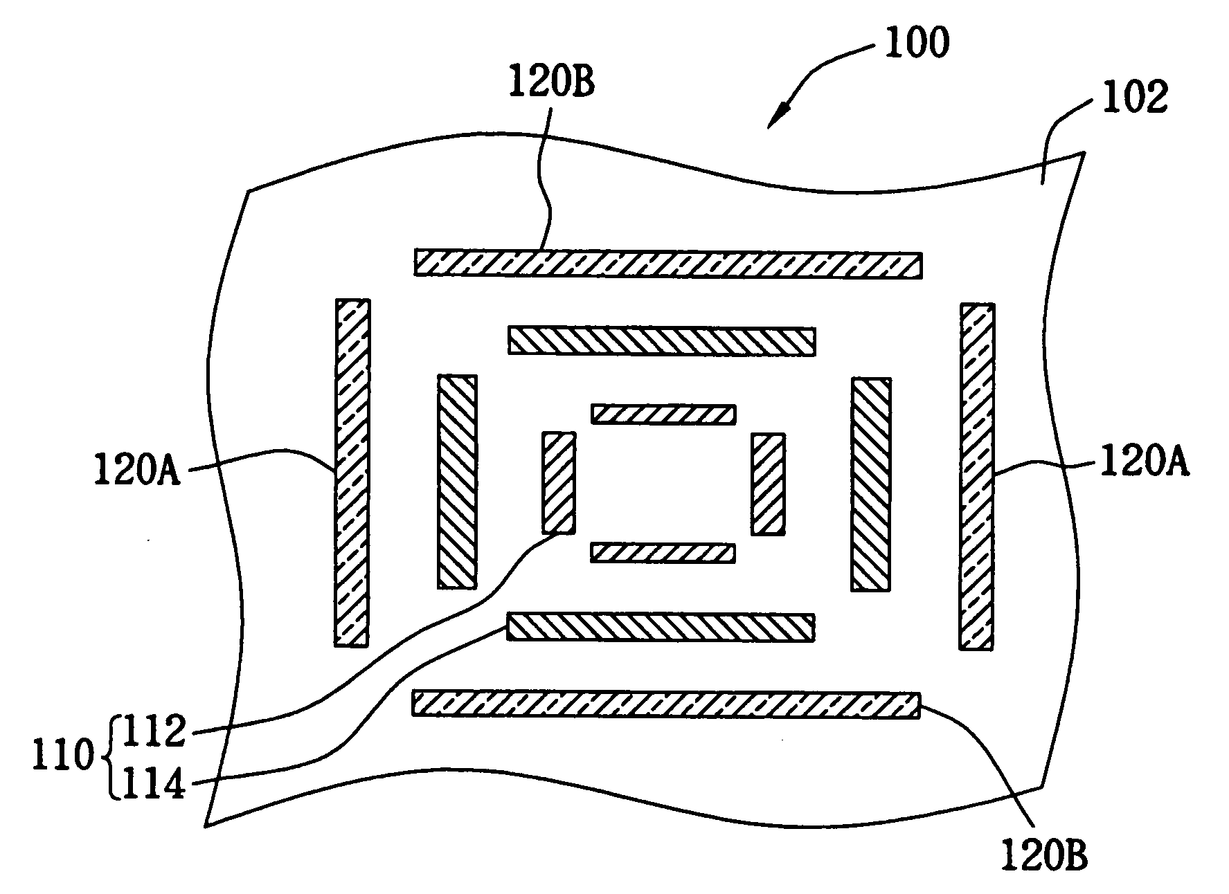
[0022]FIG. 3 is a top view of an overlay mark 100 for aligning different layers on a semiconductor wafer 102 according to the present invention. As shown in FIG. 3, the overlay mark 100 comprises a bar-in-bar mark 110 and two bar sets 120A, 120B on the semiconductor wafer 102. The bar-in-bar mark 110 comprises an inner bar mark 112 disposed on a first pre-layer and an outer bar mark 114 disposed on a second pre-layer. The inner bar mark 112 represents the pattern of a first pre-layer, and the outer bar mark 114 represents the pattern of a second pre-layer. The inner bar mark 112 comprises four bars, and the outer bar mark 114 comprises four bars outside the inner bar mark 112. The two bar sets 120A, 120B are perpendicular to each other, and each of two bar sets 120A, 120B comprises two parallel bars. The lengths of the two bar sets 120A, 120B are different, and the two bar sets 120A, 120B together form a rectangular pattern outside the bar-in-bar mark 110.
second embodiment
[0023]FIG. 4(a) to FIG. 4(d) are top views of an overlay mark 130 for aligning different layers on a semiconductor wafer 132 according to the present invention. As shown in FIG. 4(a), the lengths of the two bar set 150A, 150B are the same, and these two bar sets together form a square pattern outside a bar-in-bar mark 140 formed of an inner bar mark 142 and an outer bar mark 144. The two bar sets 150A, 150B can be positioned between the inner bar mark 142 and the outer bar mark 144, as shown in FIG. 4(b), or inside the bar-in-bar mark 140, as shown in FIG. 4(c). In addition, the bar-in-bar mark 140 and the two bar sets 150A, 150B can consist of segments patterns, as shown in FIG. 4(d).
third embodiment
[0024]FIG. 5(a) and FIG. 5(b) are top views of an overlay mark 160 for aligning different layers on a semiconductor wafer 162 according to the present invention. As shown in FIG. 5(a), the overlay mark 160 comprises a first mark 170, a second mark 180 positioned outside the first mark 170 and a third mark 190 positioned outside the second mark 180. The first mark 170 represents the pattern of a first pre-layer, the second mark 180 represents the pattern of a second pre-layer, and the third mark 190 represents the pattern of a third layer on a semiconductor wafer 162. Compared with the overlay mark 130 shown in the FIG. 4(a), the first mark 170 can be regarded as being formed of four connected inner bars, and so can the second mark 180 and the third mark 190. Besides, the first mark 170, the second mark 180 and the third mark 190 can consist of segment patterns, as shown in FIG. 5(b).
[0025] Compared with the prior technology, the present invention possesses the following advantages s...
PUM
| Property | Measurement | Unit |
|---|---|---|
| lengths | aaaaa | aaaaa |
| dimensions | aaaaa | aaaaa |
| areas | aaaaa | aaaaa |
Abstract
Description
Claims
Application Information
 - Generate Ideas
- Intellectual Property
- Life Sciences
- Materials
- Tech Scout
- Unparalleled Data Quality
- Higher Quality Content
- 60% Fewer Hallucinations
Browse by: Latest US Patents, China's latest patents, Technical Efficacy Thesaurus, Application Domain, Technology Topic, Popular Technical Reports.
© 2025 PatSnap. All rights reserved.Legal|Privacy policy|Modern Slavery Act Transparency Statement|Sitemap|About US| Contact US: help@patsnap.com


