
Method and apparatus for simplified system configuration

a technology of system configuration and simplified structure, applied in the direction of program control, total factory control, instruments, etc., can solve the problems of time-consuming and labor-intensive installation of semiconductor processing tools, the challenge of maintaining and controlling hundreds of complex manufacturing processes and machines, and the cost and tempo of developing new semiconductor devices and building new manufacturing plants

Inactive Publication Date: 2005-03-24
TOKYO ELECTRON LTD
View PDF3 Cites 9 Cited by
  • Summary
  • Abstract
  • Description
  • Claims
  • Application Information

AI Technical Summary

Problems solved by technology

The cost and tempo of developing new semiconductor devices and building new manufacturing plants is continually increasing.
Semiconductor manufacturing facilities also face the challenge of maintaining and controlling hundreds of complex manufacturing processes and machines.
Installation of a semiconductor-processing tool is a time consuming procedure.
The inefficient setup of a tool can result in facility downtimes that add to the overall operational cost.
Processing conditions change over time with the slightest changes in critical process parameters creating undesirable results.
In many cases, changes of process data reflecting deterioration of processing characteristics cannot be detected by simply referring to the process data displayed.
It is difficult to detect early stage abnormalities and characteristic deterioration of a process.

Method used


Image

  • Method and apparatus for simplified system configuration
  • Method and apparatus for simplified system configuration
  • Method and apparatus for simplified system configuration

Examples


Embodiment Construction

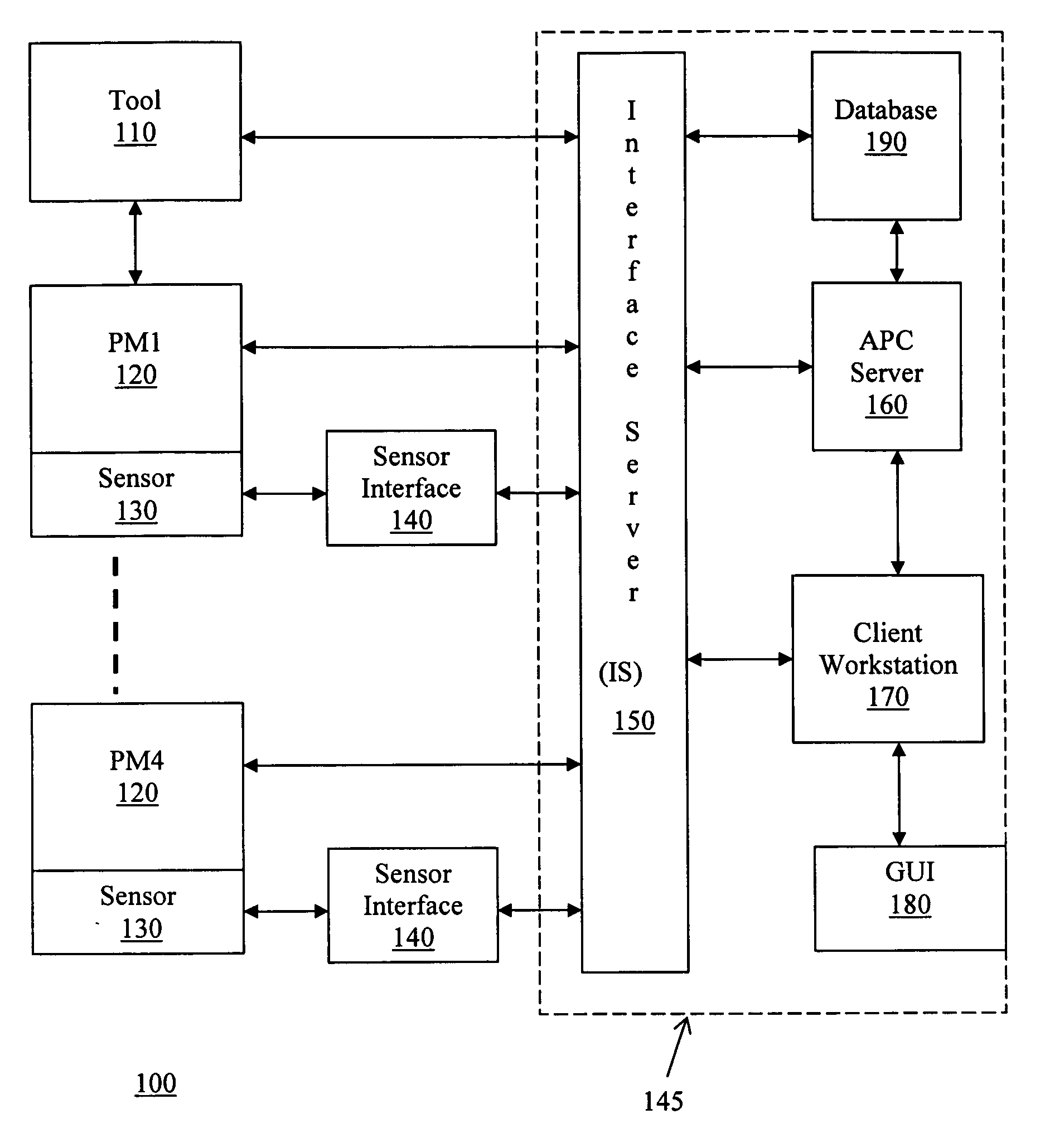
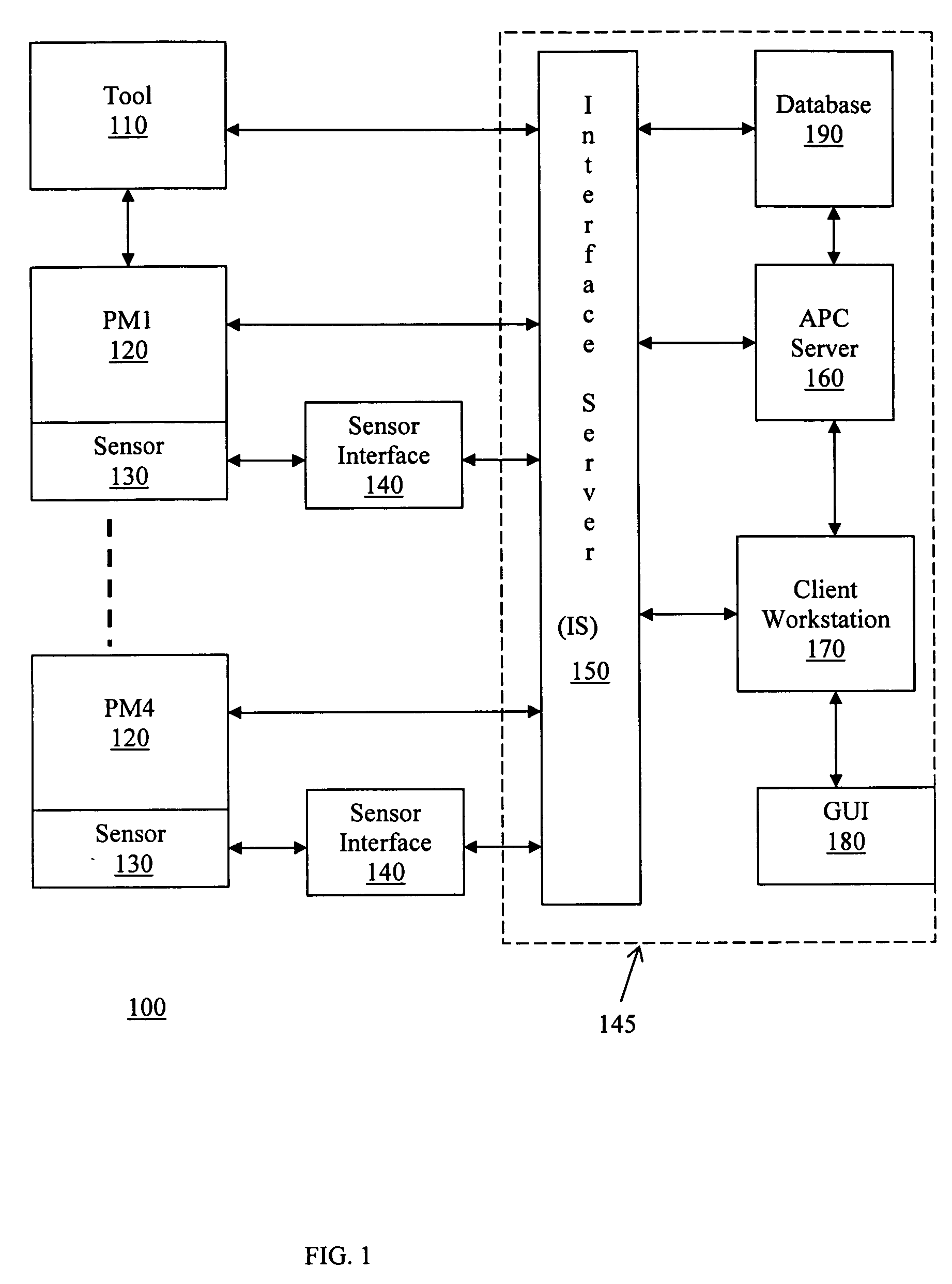
[0026]FIG. 1 shows an exemplary block diagram of an APC system in a semiconductor manufacturing environment in accordance with one embodiment of the present invention. In the illustrated embodiment, semiconductor manufacturing environment 100 comprises at least one semiconductor processing tool 110, multiple process modules 120, PM1 through PM4, multiple sensors 130 for monitoring the tool, the modules, and processes, sensor interface 140, and APC system 145. APC system 145 can comprise interface server (IS) 150, APC server 160, client workstation 170, GUI component 180, and database 190. In one embodiment, IS 150 can comprise a real-time memory database that can be viewed as a “Hub”.

[0027] In the illustrated embodiment, a single tool 110 is shown along with four process modules 120, but this is not required for the invention. The APC system 145 can interface with a number of processing tools including cluster tools having one or more process modules. The APC system can be used to ...


PUM


Abstract

A GUI is presented for configuring and initializing a semiconductor processing system, which includes a number of processing tools, a number of processing modules, a number of sensors, a number of processing models, and an alarm management system. The graphical display is organized so that all significant parameters are clearly and logically displayed so that the user is able to perform the desired configuration, initialization, and troubleshooting tasks with as little input as possible. The GUI is web-based and is viewable by a user using a web browser.

Description

CROSS-REFERENCE TO RELATED APPLICATIONS [0001] The present application is a continuation of International Application No. PCT / US03 / 10531, filed Apr. 8, 2003, which claims the benefit of, and relies for priority on, U.S. Provisional Application No. 60 / 368,162, filed on Mar. 29, 2002, the contents of both of which are herein incorporated by reference in their entireties.FIELD OF THE INVENTION [0002] The present invention is related to semiconductor processing systems, particularly to a semiconductor processing system which uses Graphical User Interfaces (GUIs) to simplify system configuration. BACKGROUND OF THE INVENTION [0003] The cost and tempo of developing new semiconductor devices and building new manufacturing plants is continually increasing. Time-to-market for new semiconductor devices is critical for the profitability and success of a company. Consumers expect the latest products and services instantaneously around the world. The need to quickly install new machines and proce...

Claims


Application Information

Patent Timeline
IPC IPC(8): G05B19/042G05B19/418H01L21/02G06F19/00
CPCG05B19/042G05B19/418G05B2219/45031G05B2219/32128G05B19/4187Y02P90/02Y02P90/80
Inventor FUNK, MERRITTCHEN, WEI
Owner TOKYO ELECTRON LTD
Learn More