
Polarization-independent optical networks in 3D photonic crystals

a technology of 3d photonic crystals and independent optical networks, applied in the field of optical communication, can solve the problems and the formation of defect bands inside the bandgap of the photonic crystal

Active Publication Date: 2005-03-10
MASSACHUSETTS INST OF TECH
View PDF2 Cites 12 Cited by
  • Summary
  • Abstract
  • Description
  • Claims
  • Application Information

AI Technical Summary

Benefits of technology

The invention provides a photonic crystal structure that includes multiple layers of rods and air holes that confine different types of polarizations. These layers create a symmetrical structure and defect bands that minimize sensitivities to polarization. The method of forming the structure involves creating slabs of rods and air holes and introducing defects to create the desired bandgap structure. Overall, this invention allows for better control over the properties of photonic crystals and improved performance in applications such as optical devices.

Problems solved by technology

The alternating slabs create a lateral symmetry plane and further include planar line defects resulting in the formation of defect bands inside the bandgap of the photonic crystal.
The method also includes forming planar line defects resulting in the formation of defect bands inside the bandgap of the photonic crystal using the slabs of dielectric rods and air holes.

Method used


Image

  • Polarization-independent optical networks in 3D photonic crystals
  • Polarization-independent optical networks in 3D photonic crystals
  • Polarization-independent optical networks in 3D photonic crystals

Examples


Embodiment Construction

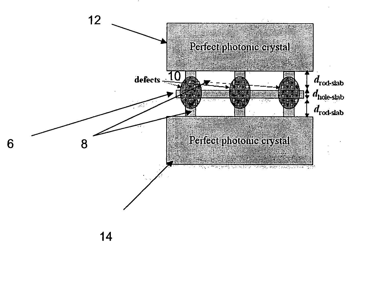
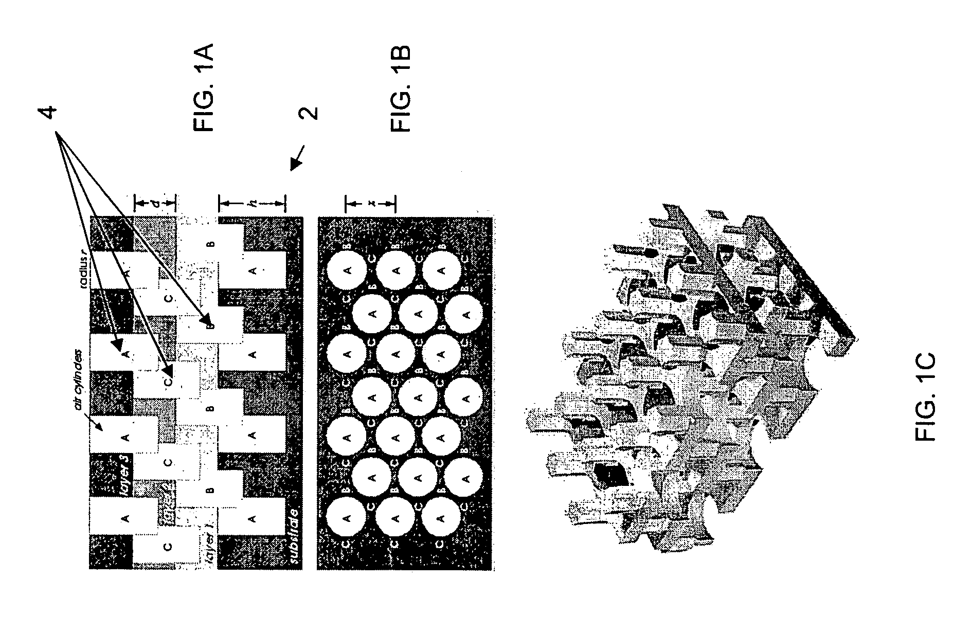
[0016] The invention addresses the issue of polarization insensitivity by employing a photonic crystal consisting of two kinds of photonic crystal slabs, each best suited for confining one of two possible polarizations: Alternating slabs of dielectric rods in air (rod layers, appropriate for confining TM-polarized waves) and air holes in dielectric (hole layers, appropriate for confining TE-polarized waves).

[0017] Wave-guiding structures can be designed within this crystal by introducing planar line defects in the hole and / or rod layers, resulting in the formation of defect (guided) bands inside the band gap. This results in planar arrays of defects, which are amenable to micro-fabrication, and is the method used here. A remarkable property of this 3D crystal is that the resulting guided modes are very similar to the 2D TE- and TM-polarized modes one gets from solving a 2D problem with the dielectric constant defined by the corresponding cross section along the defect plane. Hence,...


PUM


Abstract

A photonic crystal includes a plurality of photonic crystal slabs that is suited for confining TE polarizations and TM polarizations. The photonic crystal slabs include alternating slabs of dielectric rods and air holes. The alternating slabs create a lateral symmetry plane. The alternating slabs of dielectric rods and air holes further include planar line defects resulting in the formation of defect bands inside the bandgap of the photonic crystal.

Description

PRIORITY INFORMATION [0001] This application claims priority from provisional application Ser. No. 60 / 482,198 filed Jun. 24, 2003, which is incorporated herein by reference in its entirety.BACKGROUND OF THE INVENTION [0002] The invention relates to the field of optical communication, and in particular to integrated optical networks without polarization sensitivities. [0003] The amount of digital data processed around the globe grows rapidly every year. To perform almost any kind of operation on optical signals today (like wavelength conversion, pulse regeneration, bit-rate conversion, logic operation, etc.) the signals first need to be converted to the electronic domain. Unfortunately, there are fundamental physical reasons that prevent electronics from operating well at high frequencies. As a result, the price of electronic components grows rapidly when higher bit-rates are needed. Consequently, using all-optical signal processing becomes rapidly more and more appealing. [0004] Los...

Claims


Application Information

Patent Timeline
Patent Type & Authority Applications(United States)
IPC IPC(8): G02B6/12G02B6/126G02B6/26
CPCG02B6/1225B82Y20/00
Inventor LIDORIKIS, ELEFTERIOSJOHNSON, STEVEN G.POVINELLI, MICHELLE L.JOANNOPOULOS, JOHN D.
Owner MASSACHUSETTS INST OF TECH
Learn More