
Optical interference display panel

a display panel and optical interference technology, applied in the field of display panels, can solve the problems of inability to properly function, inhibit the light-reflection electrode from being thin, and light-related interference with other wavelengths, and achieve the effect of mitigate bad pixels

Inactive Publication Date: 2005-02-17
SNAPTRACK
View PDF74 Cites 424 Cited by
  • Summary
  • Abstract
  • Description
  • Claims
  • Application Information

AI Technical Summary

Benefits of technology

[0016] It is therefore an objective of the present invention to provide an optical interference display panel which mitigates the bad pixels caused by the defects in the optical interference reflection structure.
[0017] It is another objective of the present invention to provide an optical interference display panel which enhances the contrast of the optical interference display panel.
[0018] It is still another objective of the present invention to provide an optical interference display panel that protects an optical interference reflection structure therein from being damaged by an external environment.

Problems solved by technology

Thus, the incident visible light with the wavelength λ2 is absorbed, and the light with other wavelengths has destructive interference.
The light-reflection electrode is very thin and is easily damaged by even a tiny external force or by errors occurring during manufacturing, inhibiting it from functioning properly.
For example, the light-reflection electrode may receive defects by being touched during manufacturing or transporting procedures.
The reflected light is directly emitted outward without being filtered by the color-changeable pixel, thus causing another undesired appearance of a “light” state.
Therefore, the color-changeable pixels having defects which cause bad pixels lower the contrast and the display performance of the display panel.

Method used


Image

  • Optical interference display panel
  • Optical interference display panel
  • Optical interference display panel

Examples


Embodiment Construction

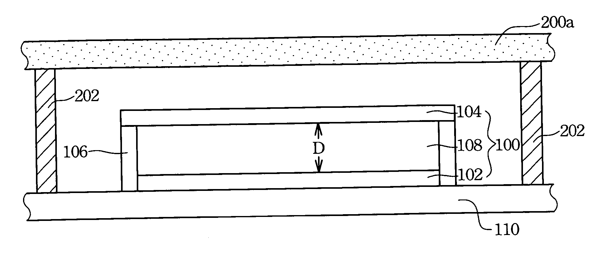
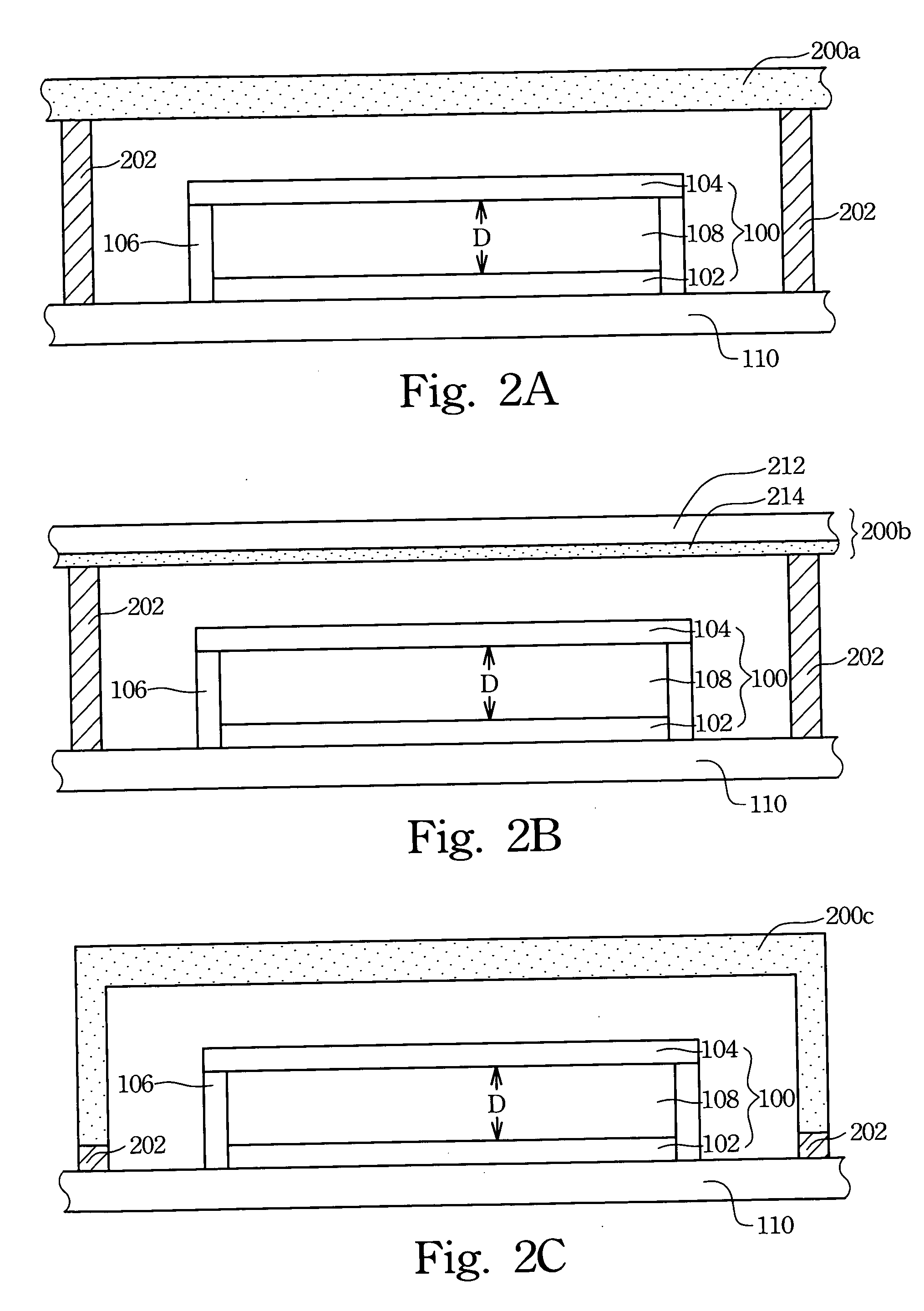
[0036] Reference will now be made in detail to the present preferred embodiments of the invention, examples of which are illustrated in the accompanying drawings. Wherever possible, the same reference numbers are used in the drawings and the description to refer to the same or like parts.

[0037] The optical interference display panel has a substrate, an optical interference reflection structure, and an opaque protection structure. The optical interference reflection structure has many color-changeable pixels and is formed on the substrate. The opaque protection structure is adhered and fixed onto the substrate with an adhesive, thus enclosing the optical interference reflection structure between the substrate and the opaque protection structure. The opaque protection structure blocks and / or absorbs light, and light thus is not emitted outward by passing through defects in the optical interference reflection structure. Moreover, the opaque protection structure and the adhesive also p...


PUM


Abstract

An optical interference display panel is disclosed that has a substrate, an optical interference reflection structure, and an opaque protection structure. The optical interference reflection structure has many color-changeable pixels and is formed on the substrate. The opaque protection structure is adhered and fixed onto the substrate with an adhesive and encloses the optical interference reflection structure between the substrate and the opaque protection structure. The opaque protection structure blocks and / or absorbs light, and light is thus not emitted outward by passing through defects in the optical interference reflection structure. Moreover, the opaque protection structure and the adhesive also prevent the optical interference reflection structure from being damaged by an external environment.

Description

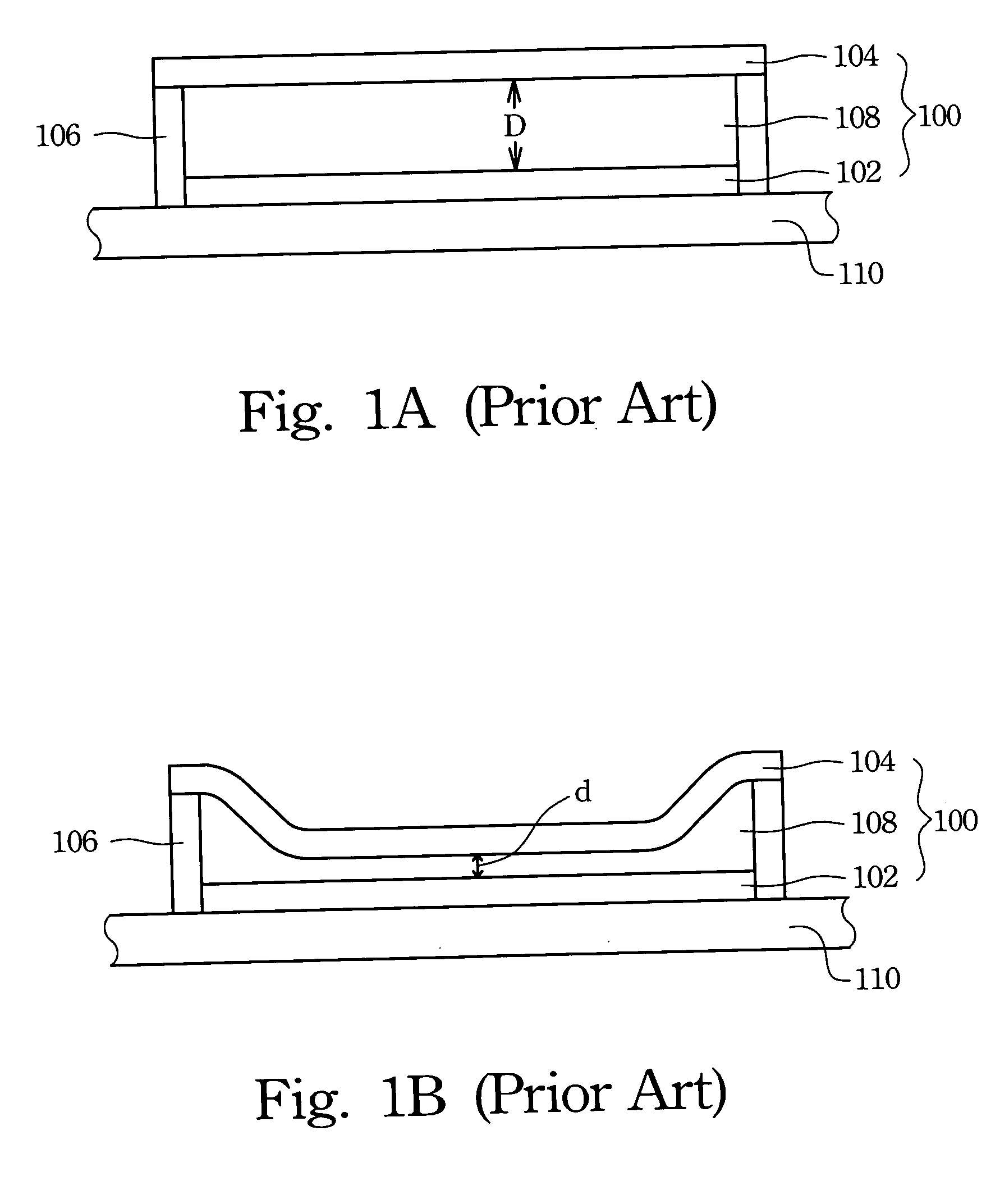
BACKGROUND [0001] 1. Field of Invention [0002] The present invention relates to a display panel. More particularly, the present invention relates to an optical interference display panel. [0003] 2. Description of Related Art [0004] Due to being lightweight and small in size, a display panel is favorable in the market of portable displays and displays with space limitations. To date, in addition to liquid crystal display (LCD), organic light emitting diode (OLED) and plasma display panel (PDP) modules, a module of the optical interference display has been investigated. [0005] U.S. Pat. No. 5,835,255 discloses a modulator array, that is, a color-changeable pixel for visible light which can be used in a display panel. FIG. 1A illustrates a cross-sectional view of a prior art modulator. Every modulator 100 comprises two walls, 102 and 104. These two walls are supported by posts 106, thus forming a cavity 108. The distance between these two walls, the depth of cavity 108, is D. The wall ...

Claims


Application Information

Patent Timeline
IPC IPC(8): G02B26/00G02B26/08H05B33/00H05B33/04
CPCG02B26/001G02B26/08
Inventor TSAI, HSIUNG-KUANG
Owner SNAPTRACK
Learn More