
Method and system for compression of address tags in memory structures

a memory structure and address tag technology, applied in the field of computer systems, can solve the problems of affecting the cost factor of processing units, requiring sophisticated cooling techniques, and low yield

Inactive Publication Date: 2003-12-04
SUN MICROSYSTEMS INC
View PDF11 Cites 12 Cited by
  • Summary
  • Abstract
  • Description
  • Claims
  • Application Information

AI Technical Summary

Benefits of technology

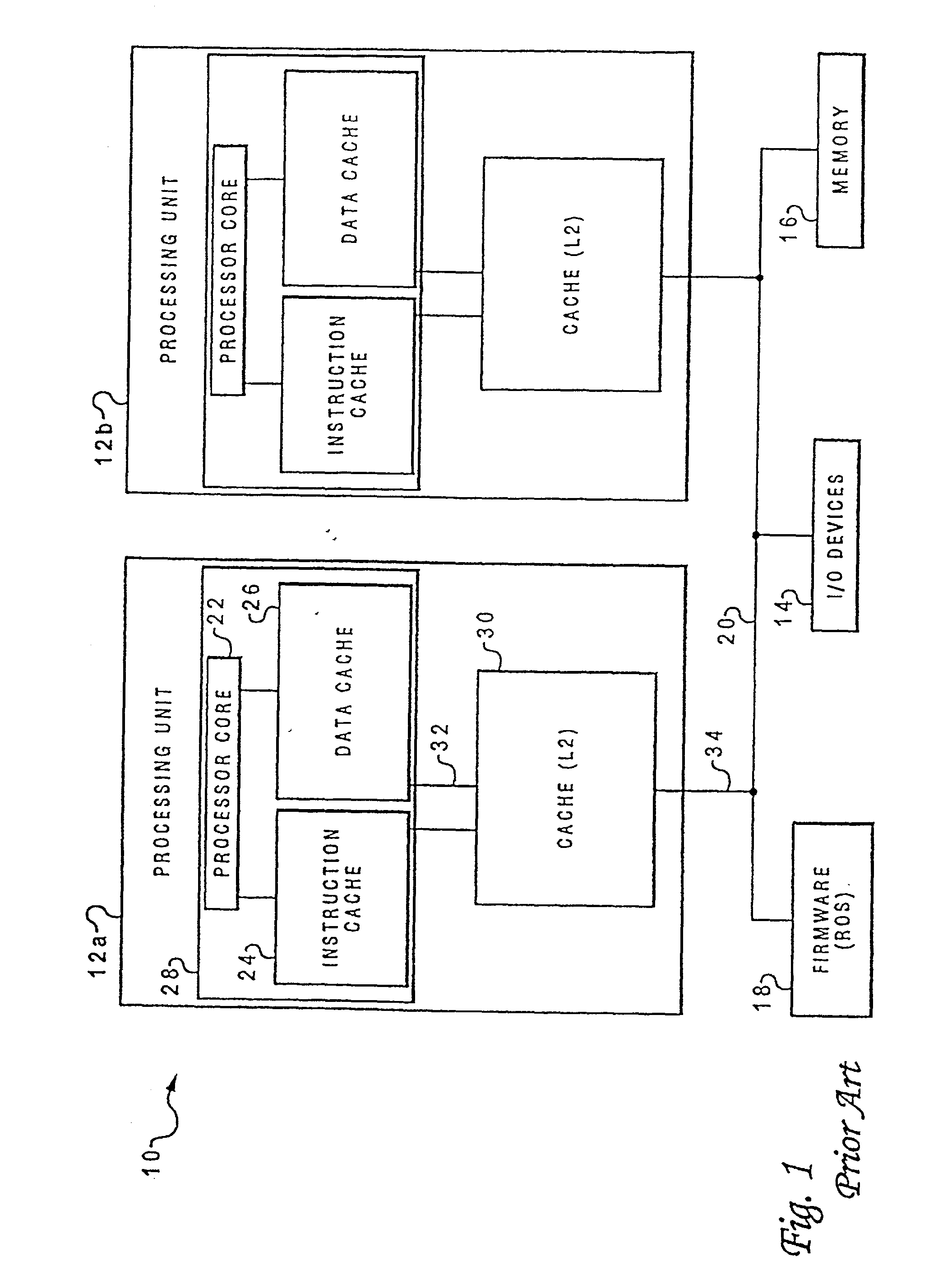
0019] FIG. 1 is a block diagram of a conventional computer system having ...

Problems solved by technology

An increase in cache area results in lower yields, while an increase in power consumption requires sophisticated cooling techniques to retain performance and reliability.
Both of these problems significantly affect the cost factor for processing units.
These problems occur not just with caches, but also with many other structures that require address tags.
Since the corrupted load data may have been used by a dependent instruction, all instructions previous to the load instruction must be restarted, with a resulting degradation in performance.
CAMs are thus particularly power-hungry structures, which can exacerbate the foregoing problems.

Method used


Image

  • Method and system for compression of address tags in memory structures
  • Method and system for compression of address tags in memory structures
  • Method and system for compression of address tags in memory structures

Examples


Embodiment Construction

)

[0025] The present invention is directed to a method and system for compressing address tags in memory structures of a computer. By compressing the address tags, fewer bits are required for storage, and for searching or hit / miss comparison. The memory structures can thus be reduced in size, and operate with less power.

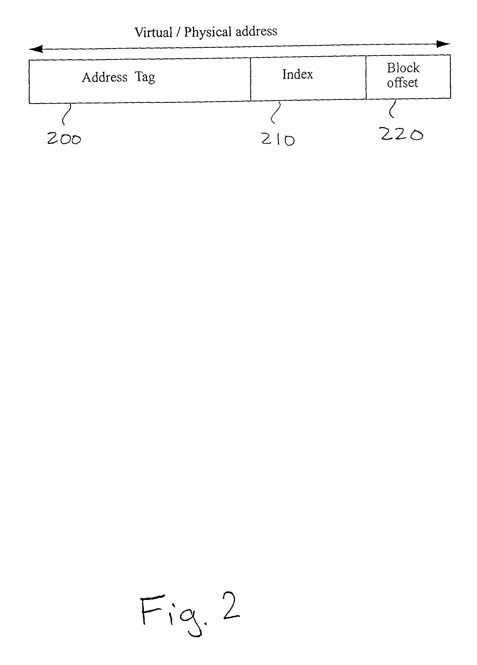
[0026] One exemplary memory structure in which the invention may be embodied is a cache. As explained in the Background section, caches generally have two arrays: the actual values or cache entries, and the address tags or directory. For a 64-kilobyte (KB), direct-mapped data cache that is virtually indexed and virtually tagged, which uses 32-bit virtual addressing, and a block size of four bytes, the total size of a typical prior art cache is 98 KB, including the cache directory (and validity bits). The tags occupy 34 KB, or about 50% of the size of the cache entry array. Though this percentage may be reduced with larger block sizes, it nevertheless constitutes a sig...


PUM


Abstract

A memory structure of a computer system receives an address tag associated with a computational value, generates a modified address which corresponds to the address tag using a compression function, and stores the modified address as being associated with the computational value. The address tag can be a physical address tag or a virtual address tag. The computational value (i.e., operand data or program instructions) may be stored in the memory structure as well, such as in a cache associated with a processing unit of the computer system. For such an implementation, the compressed address of a particular cache operation is compared to existing cache entries to determine which a cache miss or hit has occurred. In another exemplary embodiment, the memory structure is a memory disambiguation buffer associated with at least one processing unit of the computer system, and the compressed address is used to resolve load / store collisions. Compression may be accomplished using various encoding schemes, including complex schemes such as Huffinan encoding, or more elementary schemes such as differential encoding. The compression of the address tags in the memory structures allows for a smaller tag array in the memory structure, reducing the overall size of the device, and further reducing power consumption.

Description

[0001] 1. Field of the Invention[0002] The present invention generally relates to computer systems and, more particularly, to a method of handling address tags used by memory structures of a computer system, such as system memory, caches, translation lookaside buffers, or memory disambiguation buffers.[0003] 2. Description of the Related Art[0004] The basic structure of a conventional computer system 10 is shown in FIG. 1. Computer system 10 may have one or more processing units, two of which 12a and 12b are depicted, which are connected to various peripheral devices, including input / output (I / O) devices 14 (such as a display monitor, keyboard, and permanent storage device), memory device 16 (such as random access memory or RAM) that is used by the processing units to carry out program instructions, and firmware 18 whose primary purpose is to seek out and load an operating system from one of the peripherals (usually the permanent memory device) whenever the computer is first turned ...

Claims


Application Information

Patent Timeline
IPC IPC(8): G06F12/08G06F12/10
CPCG06F12/0802Y02B60/1225G06F12/1027G06F12/02G06F2212/401Y02D10/00
Inventor VENKATRAO, BALAKRISHNATHATIPELLI, KRISHNA M.
Owner SUN MICROSYSTEMS INC
Learn More