Active matrix substrate
a technology of active matrix and substrate, which is applied in the direction of identification means, instruments, semiconductor devices, etc., can solve the problems of difficult formation of oxide semiconductor tft having both characteristics, and achieve the effect of suppressing the characteristic of the circuit
- Summary
- Abstract
- Description
- Claims
- Application Information
AI Technical Summary
Benefits of technology
Problems solved by technology
Method used
Image
Examples
embodiment 1
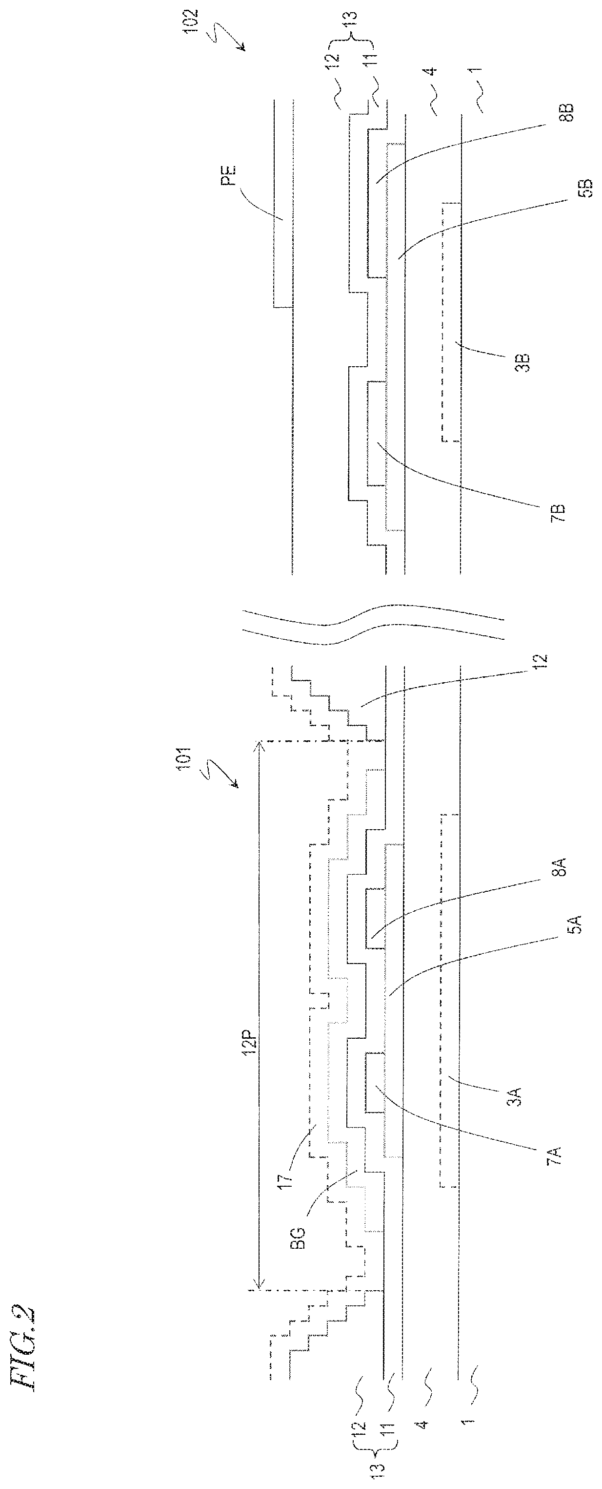
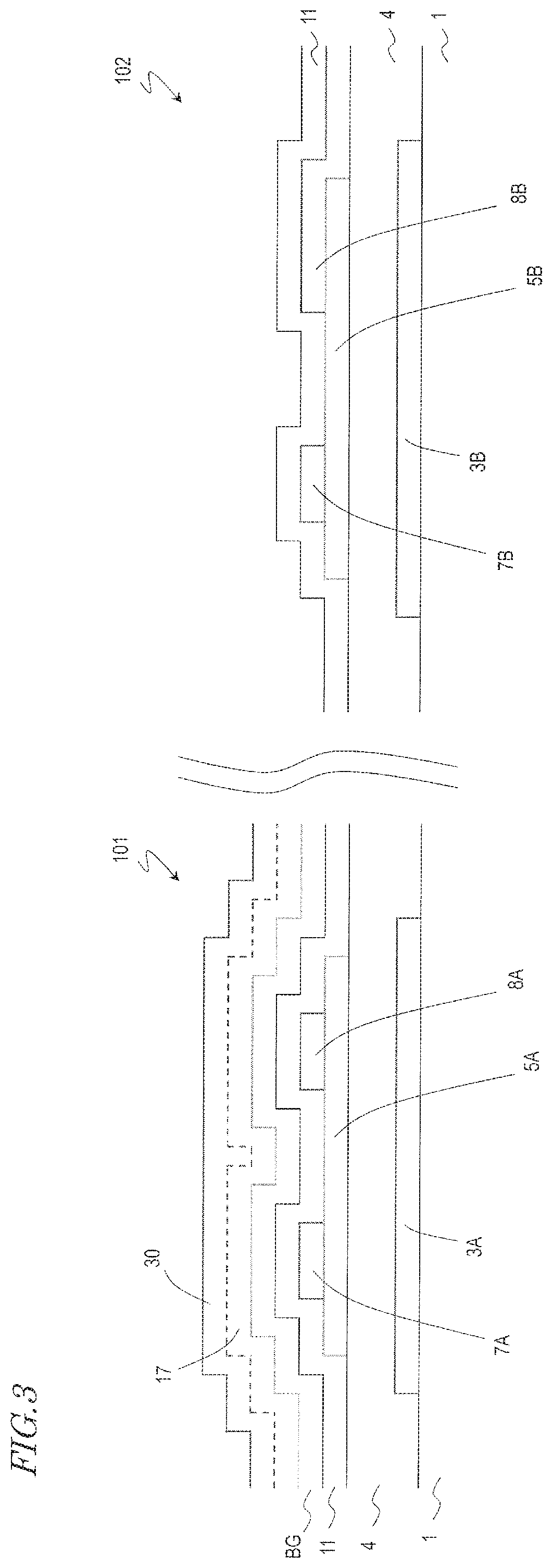
[0097]Hereinafter, embodiment 1 of the active matrix substrate according to the present invention will be described with reference to the drawings. The active matrix substrate according to this embodiment is widely applicable to a liquid crystal display apparatus, an organic EL display device, an inorganic EL display device or the like.
[0098]FIG. 7 is a schematic plan view illustrating an active matrix substrate 1001 according to this embodiment.
[0099]The active matrix substrate 1001 includes a display region 800 including a plurality of pixel regions and a region 900 other than the display regions 800 (non-display region). The “pixel region” is a region corresponding to a pixel in a display device, and in this specification, may be referred to simply as a “pixel”.
[0100]In the display region 800, a plurality of gate lines GL and a plurality of source lines SL are formed. Each of regions defined by these lines is the “pixel”. A plurality of such pixels are located in a matrix. In eac...
embodiment 2
[0156]In an active matrix substrate according to embodiment 2, the upper transparent electrode acts as the common electrode CE and the lower transparent electrode acts as the pixel electrode PE, unlike in the active matrix substrate according to embodiment 1. In this embodiment, the back-gate electrode BG of the first TFT is formed of the same transparent conductive film as that of the pixel electrode PE, and the shield layer 30 is formed of the same transparent conductive film as that of the common electrode CE.
[0157]FIG. 13 is a schematic plan view showing an active matrix substrate 1004 according to this embodiment as an example. FIG. 14(a) and FIG. 14(b) are each a schematic cross-sectional view of the active matrix substrate 1004, and respectively show cross-sectional structures taken along lines A-A and B-B in FIG. 13. In FIG. 13 and FIG. 14, elements substantially the same as those in FIG. 8 through FIG. 10 bear the identical reference signs thereto. In the following, differe...
embodiment 3
[0170]In an active matrix substrate according to embodiment 3, the interlayer insulating layer 13 includes no organic insulating layer, unlike in the active matrix substrate according to embodiment 1 or 2.
[0171]FIG. 15 is a schematic plan view showing an active matrix substrate 1005 according to this embodiment as an example. FIG. 16(a) and FIG. 16(b) are each a schematic cross-sectional view of the active matrix substrate 1005, and respectively show cross-sectional structures taken along lines A-A and B-B in FIG. 15. In FIG. 15 and FIG. 16, elements substantially the same as those in FIG. 8 through FIG. 14 bear the identical reference signs thereto. In this embodiment, an example in which the upper transparent electrode acts as the common electrode CE and the lower transparent electrode acts as the pixel electrode PE will be described. Alternatively, the upper transparent electrode may act as the pixel electrode PE and the lower transparent electrode may act as the common electrode...
PUM
| Property | Measurement | Unit |
|---|---|---|
| gate voltage Vg | aaaaa | aaaaa |
| distance | aaaaa | aaaaa |
| thickness | aaaaa | aaaaa |
Abstract
Description
Claims
Application Information
 - R&D
- Intellectual Property
- Life Sciences
- Materials
- Tech Scout
- Unparalleled Data Quality
- Higher Quality Content
- 60% Fewer Hallucinations
Browse by: Latest US Patents, China's latest patents, Technical Efficacy Thesaurus, Application Domain, Technology Topic, Popular Technical Reports.
© 2025 PatSnap. All rights reserved.Legal|Privacy policy|Modern Slavery Act Transparency Statement|Sitemap|About US| Contact US: help@patsnap.com


