Flexible printed circuit board

a printed circuit board and flexible technology, applied in printed circuit aspects, high frequency circuit adaptations, cross-talk/noise/interference reduction, etc., can solve the problems of reducing the effect of adjusting assembly tolerances reducing the flexibility of flexible printed circuit boards, and reducing the number of layers. , to achieve the effect of maintaining flexibility and low-reflection connection

Active Publication Date: 2020-06-16
DALIAN CANGLONG OPTOELECTRONICS TECH
View PDF4 Cites 0 Cited by
  • Summary
  • Abstract
  • Description
  • Claims
  • Application Information

AI Technical Summary

Benefits of technology

[0007]An object of the present invention is to achieve a low-reflection connection of a flexible printed circuit board while maintaining flexibility without increasing the number of layers.
[0022]Compared with the prior art, the present invention is able to realize a low-reflection connection of a flexible printed circuit board while maintaining flexibility without increasing the number of layers, so as to meet the requirements of the bandwidth (S21) and reflection (S11) of high-speed signals, and obtain the low reflection characteristic of −20 dB or less up to 40 GHz.

Problems solved by technology

However, in order to achieve the reflection performance of 40 GHz, both of the third patent document and the fourth patent document increase the number of layers of the flexible printed circuit board, which makes the flexibility of the flexible printed circuit board lower, the bending becomes difficult, and the effect of adjusting assembly tolerances of the flexible printed circuit board is reduced.
When the assembly is misaligned, stress is easily generated, causing the pads to be torn, thereby invalidating the product.

Method used


Image

  • Flexible printed circuit board
  • Flexible printed circuit board
  • Flexible printed circuit board

Examples


Embodiment Construction

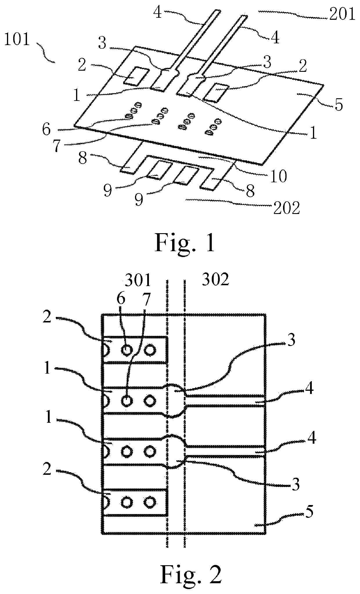
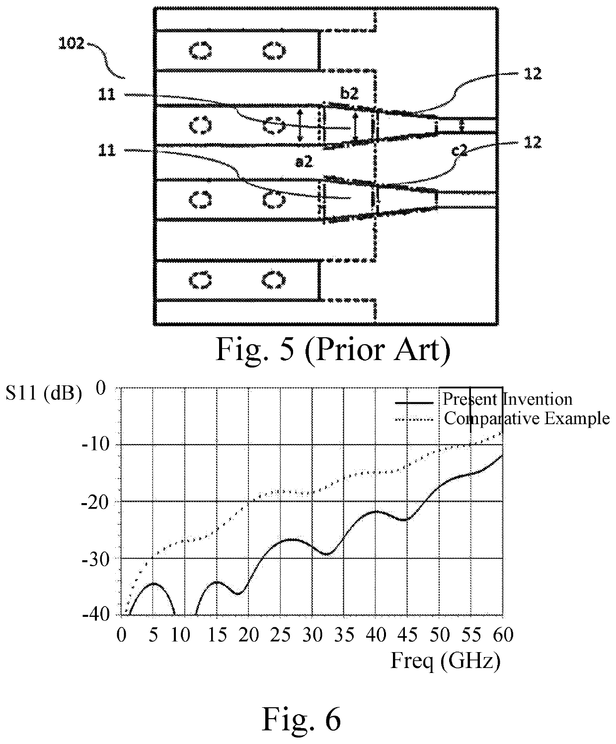
[0030]As shown in FIGS. 1 to 4 of the drawings, a flexible printed circuit board 101 provided by the present invention has a first conductor layer 201, a second conductor layer 202 and a dielectric layer 5 sandwiched between the first conductor layer 201 and the second conductor layer 202.

[0031]According to the present invention, the flexible printed circuit board 101 comprises a pad portion 301 for electrically connecting with an external device and a wire portion 302 for transmitting signals. The wire portion 302 is a differential circuit constructed with microstrip lines which comprises a pair of signal wires 4 formed in the first conductor layer 201 and a grounding layer 10 formed in the second conductor layer 202. The pad portion 301 comprises a pair of first signal pads 1 and a pair first grounding pads 2 all of which are formed in the first conductor layer 201, and a pair of second signal pads 9 and a pair of second grounding pads 8 all of which are formed in the second condu...


PUM


Abstract

A flexible printed circuit board is disclosed, which includes a pad portion, wherein the pad portion includes a pair of first signal pads formed in a first conductor layer and respectively connected with a pair of signal wires, a pair of second signal pads formed in a second conductor layer and electrically separated from a grounding layer; a pair of first grounding pads formed in the first conductor layer and electrically separated from the pair of signal wires, wherein: the pair of first signal pads is sandwiched between the pair of first grounding pads, and a pair of second grounding pads formed in the second conductor layer and connected with the grounding layer, wherein the pair of second signal pads are sandwiched between the pair of second grounding pads. A width of the first and the second signal pads is larger than that of the signal wires.

Description

CROSS REFERENCE OF RELATED APPLICATION[0001]This is a U.S. National Stage under 35 U.S.C 371 of the International Application PCT / CN2017 / 087151, filed Jun. 5, 2017, which claims priority under 35 U.S.C. 119(a-d) to CN 201710080992.7, filed Feb. 15, 2017.BACKGROUND OF THE PRESENT INVENTIONField of Invention[0002]The present invention relates to a flexible printed circuit board.Description of Related Arts[0003]In the existing optical transceiver module, the transmission rate of high-speed signals is increased from several hundred Mbps to several tens of Gbps. Inside the optical transceiver module, a printed circuit board assembly (PCBA) and a light receiving and transmitting device need to be connected by a flexible printed circuit (ITC) for adjusting assembly tolerances inside the entire optical transceiver module.[0004]This also requires that the signal design of the flexible printed circuit board needs to meet the requirements of the bandwidth (S21) and reflection (S11) of high-spe...

Claims


Application Information

Patent Timeline
Patent Type & Authority Patents(United States)
IPC IPC(8): H05K1/14H05K1/02H05K1/11
CPCH05K1/118H05K1/0251H05K2201/09672H05K2201/094H05K2201/09727H05K2201/09609H05K1/0218H05K1/0245H05K2201/09372H05K1/0227H05K2201/09618
Inventor WANG, HAOZHANG, SHUNCUI, LINZHANG, WENCHENLIAO, CHUANWU
Owner DALIAN CANGLONG OPTOELECTRONICS TECH
Why Eureka
Try Eureka