Structure of flexible printed circuit board

一种柔性印制、电路板的技术,应用在印刷电路、印刷电路、印刷电路零部件等方向,能够解决焊盘撕裂、降低柔性印制电路板调整组装公差的作用、产品失效等问题

Active Publication Date: 2017-08-18
DALIAN CANGLONG OPTOELECTRONICS TECH
View PDF7 Cites 11 Cited by
  • Summary
  • Abstract
  • Description
  • Claims
  • Application Information

AI Technical Summary

Problems solved by technology

[0005] However, in order to achieve the reflection performance of 40 GHz, patent documents 3 and 4 increase the number of layers of the flexible printed circuit board, which will reduce the flexibility of the flexible printed circuit board, make it difficult to bend, and reduce the adjustment and assembly of the flexible printed circuit board. The role of tolerance
When the assembly is misplaced, it is easy to generate stress, causing the pad to tear and making the product fail

Method used


Image

  • Structure of flexible printed circuit board
  • Structure of flexible printed circuit board
  • Structure of flexible printed circuit board

Examples


Embodiment 1

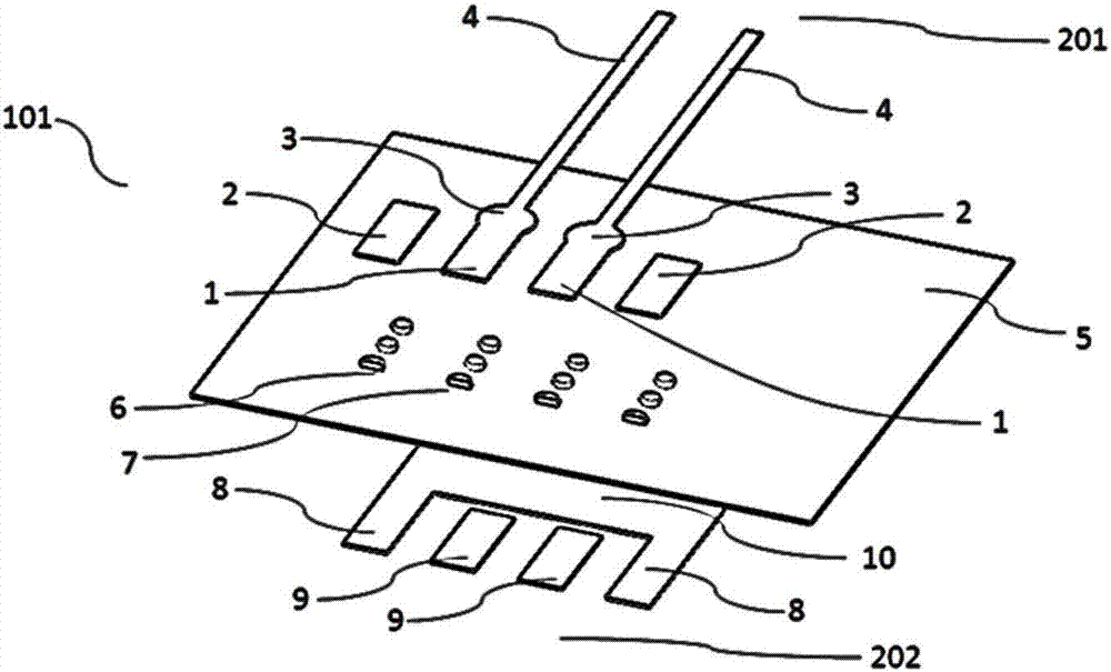
[0021] Such as Figure 1-4 As shown, the flexible printed circuit board 101 of the present invention has a structure of a first conductor layer 201 , a second conductor layer 202 and a dielectric layer 5 .

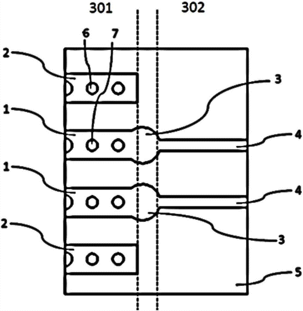
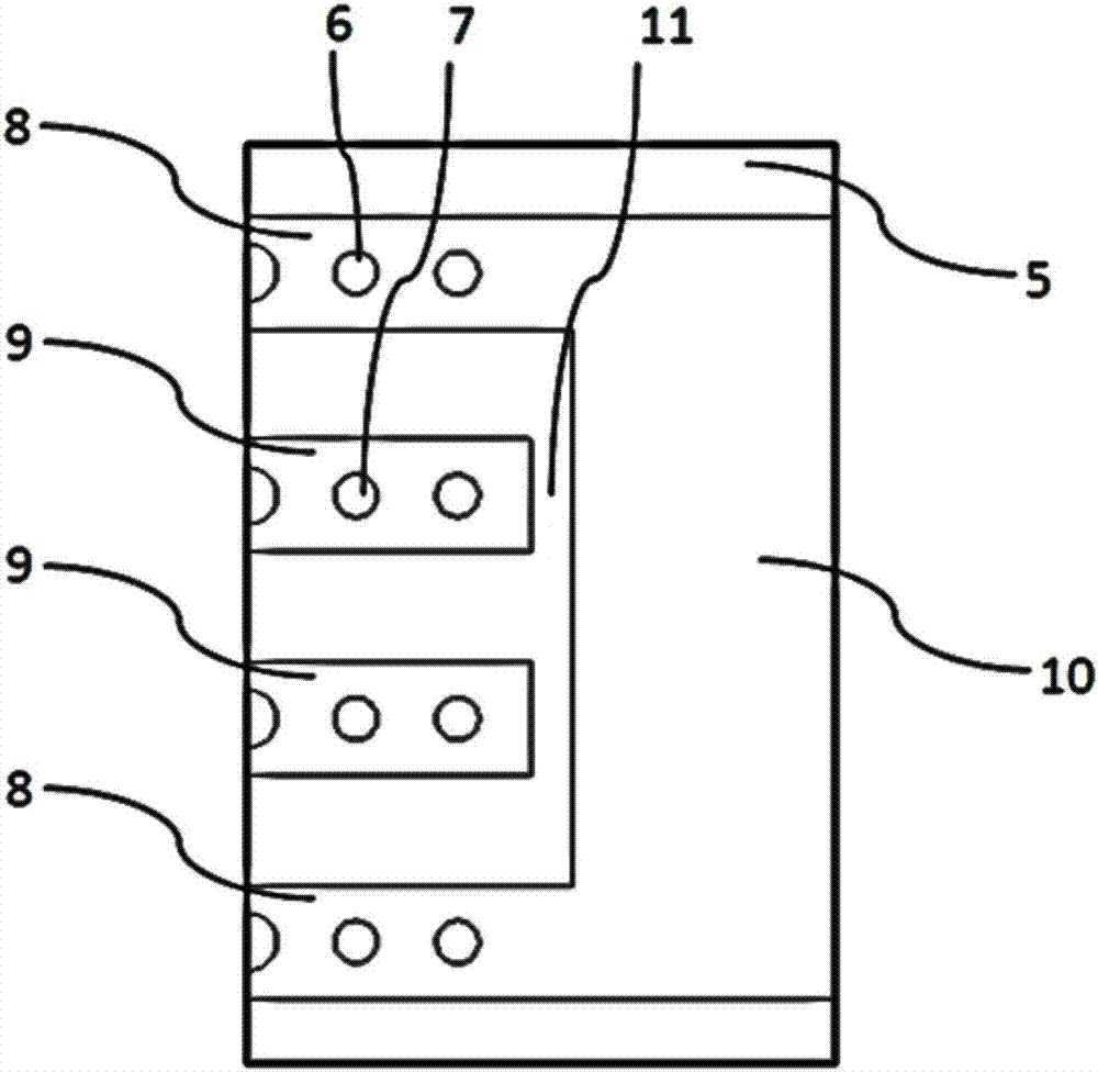
[0022] The flexible printed circuit board 101 of the present invention has a pad portion 301 electrically connected to the outside, and a line portion 302 for transmitting signals. The line portion 302 is a differential line of a microstrip line formed between the signal line 4 of the first conductor layer 201 and the ground layer 10 of the second conductor layer 202 . The pad part 301 is composed of the first signal pad 1 and the first ground pad 2 on the first conductor layer 201 , and the second signal pad 9 and the second ground pad 8 on the second conductor layer 202 . The electrical connection between the first signal pad 1 and the second signal pad 9 is realized through the signal pad via hole 7 . The first ground pad 2 and the second ground pad 8 are electrically...

Embodiment 2

[0025] The structure of the flexible printed circuit board in this embodiment is basically the same as that in Embodiment 1, except that the flexible printed circuit board 101 exists between the pad portion 301 and the line portion 302 of the first conductor layer 201 Next to the conductor transition area 3, the conductor transition area 3 is located between the first signal pad and its corresponding signal line, and the conductor width in the conductor transition area changes as follows: it first becomes wider than the first signal pad, It is then narrowed to the same width as the signal line. Between the pad portion 301 and the line portion 302 of the second conductor layer 202 there is a gap 11 for electrically separating the signal pad and the ground layer.

[0026] From Figure 4 From the perspective view of the flexible printed circuit board, it can be seen that the conductor transition zone 3 is located just above the electrical separation gap for compensating its impe...


PUM


Abstract

The invention relates to a structure of a flexible printed circuit board. Disclosed by the invention is the structure of a flexible printed circuit board. The structure is provided with a bonding pad portion used for acquiring electrical connection with other circuit substrates, and is characterized in that the bonding pad portion is provided with first signal bonding pads, second signal bonding pads, a pair of first grounding bonding pads and a pair of second grounding bonding pads; the first signal bonding pads are formed in a first conductor layer in a mode of being connected with signal lines respectively; the second signal bonding pads are formed in a second conductor layer and electrically separated from a grounding layer; the pair of first grounding bonding pads are formed in the first conductor layer, electrically separated from the signal lines and configured to clamp the first signal bonding pads from the left and right sides respectively; and the pair of second grounding bonding pads are formed in the second conductor layer, connected with the grounding layer and configured to clamp the second signal bonding pads from the left and right sides respectively. The first signal bonding pads and the second signal bonding pads are wider than the signal lines. Compared with the prior art, the structure can realize low-reflection connection of the flexible printed circuit board under the condition of keeping the flexibility unchanged and not increasing the number of layers.

Description

technical field [0001] The invention relates to a structure of a flexible printed circuit board. Background technique [0002] In existing optical transceiver modules, the transmission rate of high-speed signals has been increased from hundreds of Mbps to tens of Gbps. Inside the optical transceiver module, the printed circuit board assembly (Printed Circuit Board Assembly: PCBA) and the optical receiving and emitting devices need to be connected by a flexible printed circuit board (Flexible Printed Circuit: FPC) to adjust the entire optical transceiver Assembly tolerances within the module. [0003] This also requires the signal design of the flexible printed circuit board to meet the bandwidth (S21) and reflection (S11) requirements of tens of Gbps high-speed signals. A flexible printed circuit board generally has a flexible base material, and has a transmission line constructed of a microstrip line or a strip line composed of a signal line and a ground layer. In the op...

Claims


Application Information

Patent Timeline
Patent Type & Authority Applications(China)
IPC IPC(8): H05K1/02H05K1/11
CPCH05K1/0218H05K1/0245H05K1/118H05K2201/09372H05K2201/09672H05K1/0251H05K2201/09727H05K1/0227H05K2201/09618H05K2201/094H05K2201/09609
Inventor 王昊张舜崔琳张文臣廖传武
Owner DALIAN CANGLONG OPTOELECTRONICS TECH
Why Eureka
Try Eureka